Plasma display panel
a display panel and plasma technology, applied in the field of plasma display panels, can solve the problems of increasing the discharge distance between the first display electrode and the address electrode, and consuming more power, so as to reduce the address voltage, improve the emission efficiency, and reduce the sustain discharge voltage
- Summary
- Abstract
- Description
- Claims
- Application Information
AI Technical Summary
Benefits of technology
Problems solved by technology
Method used
Image
Examples
Embodiment Construction
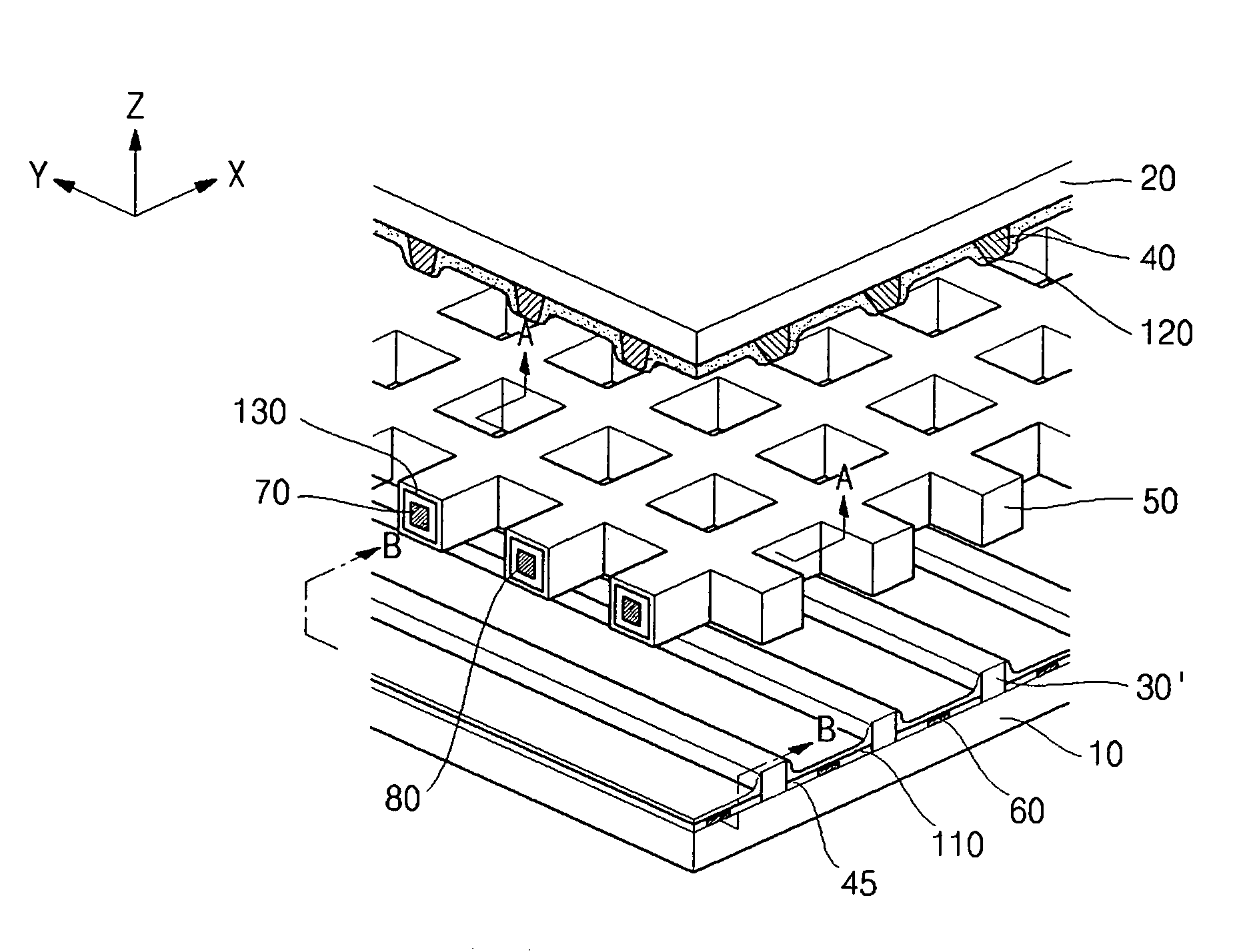
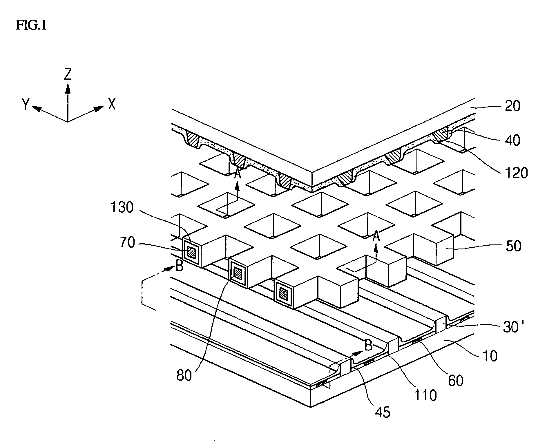
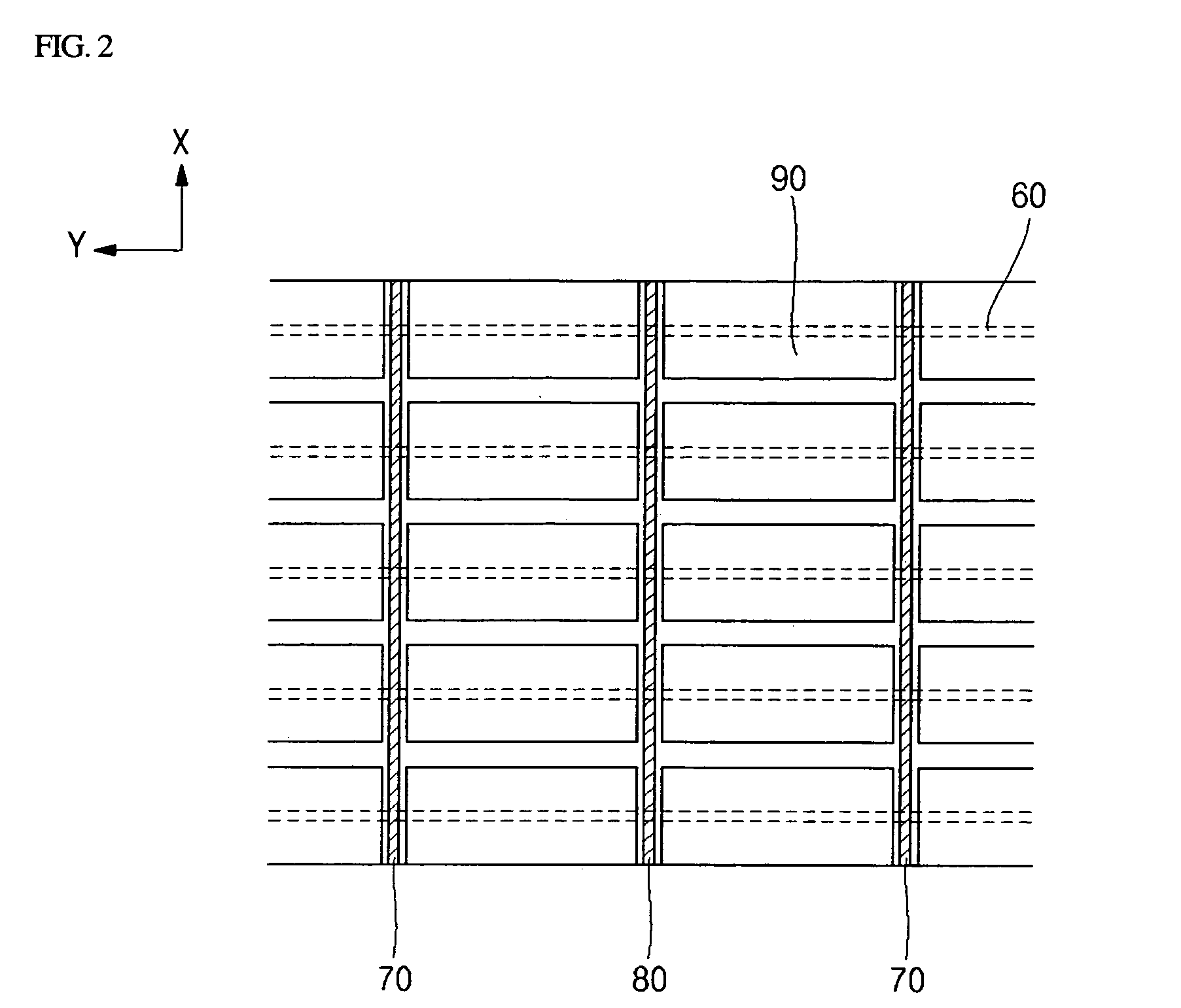
[0032]A plasma display panel according to a first embodiment of the present invention, referring to FIGS. 1, 2 and 3a, includes a first substrate (hereinafter, referred to as rear substrate) 10, a second substrate (hereinafter, referred to as front substrate) 20, a rear barrier layer 30, a front barrier layer 55, first display (Y) electrodes 70, second display (X) electrodes 80, and address (A) electrodes 60. The rear barrier layer 30 includes first barriers 30′ and delimits a number of discharge cells 90. The front barrier layer 55 includes second barriers 40 and third barriers 50. First, second, and third fluorescent substance layers 110, 120, 130 are formed on the first, second, and third barriers 30′, 40, 50, respectively. The discharge cells 90 are provided with fluorescent substance layers for absorbing vacuum UV rays and emitting visible rays and are filled with discharge gas for generating vacuum UV rays by means of plasma discharge.
[0033]The rear substrate 10 is made of a p...
PUM
 Abstract
Description
Claims
Application Information


