Thermal infrared solid state imaging device and infrared camera

a solid-state imaging and infrared technology, applied in the field of infrared solid-state imaging devices and infrared cameras, can solve the problems of increased discharge, difficult low-voltage drive, and particularly pronounced problems, and achieve the effects of low noise, shortening integration time, and high gain

Active Publication Date: 2010-05-18
MITSUBISHI ELECTRIC CORP
View PDF12 Cites 16 Cited by
  • Summary
  • Abstract
  • Description
  • Claims
  • Application Information

AI Technical Summary

Benefits of technology

[0022]According to the invention, a holding capacitor connected to the gate of the bias current supply transistor holds the gate voltage of a bias current supply transistor that is required to supply a current flowing depending on the signal input to the integrating transistor when the gate connection switch is on, and the input-converted gate voltage corresponding to the 1 / f noise current at this time. When the gate connection switch turns off and the input voltage of the integrating transistor then changes from the voltage when the gate connection switch is on, the change in the integrating transistor current caused by this change flows to the integrating capacitor that is AC coupled at the output coupling capacitor and is integrated. It is therefore not necessary to set the bias voltage in order to set the bias current, and a bias current does not flow to the integrating capacitor. High gain and low noise can therefore be achieved without setting a high integrating capacitor reset voltage or shortening the integration time.
[0023]In addition, by providing a reference pixel (non-heat-insulated pixel) that provides an output according to the ambient temperature change without sensing infrared light, and inputting the output of the reference pixel to the integrating transistor when the gate connection switch is on, the bias current is set according to pixel output based on the ambient temperature change. Only the signal current equal to the difference between the reference pixel and the normal pixels is therefore integrated. More specifically, variation in the output due to change in the ambient temperature can be reduced.

Problems solved by technology

Some problems with the thermal infrared solid state imaging device taught in the non-patent document 1 are described below.(1) Low voltage drive is difficult because the potential of the integrating capacitor Cin is discharged from the reset voltage Vref during the integration period even in the incident infrared state used as the reference.
This problem is particularly pronounced because discharge increases if the bias current is increased to increase sensitivity and increase the gain of the integration circuit, or if the integration time is increased to reduce noise.(2) The source voltage Vss of the integrating transistor is necessary.
This problem can be reduced by such measures as setting the threshold voltage sufficiently high, reducing the pixel current, or reducing the drive line resistance, but the sensitivity deviation cannot be reduced to zero.
The integration circuit gain that is proportional to the integration time therefore drops, the noise bandwidth that is proportional to the integration time increases, and noise is greater than conventionally.(2) While suppressing signal variation due to threshold voltage variation in the integrating transistor is an important feature, a long time is required for sampling the threshold voltage of the integrating transistor because the current of the integrating transistor tends to be cut-off.
The prior art thus cannot sample the threshold voltage during the horizontal blanking period, and the benefit of sampling during this period cannot be achieved.

Method used


Image

  • Thermal infrared solid state imaging device and infrared camera
  • Thermal infrared solid state imaging device and infrared camera
  • Thermal infrared solid state imaging device and infrared camera

Examples


embodiment 1

1. Structure of Thermal Infrared Solid State Imaging Device

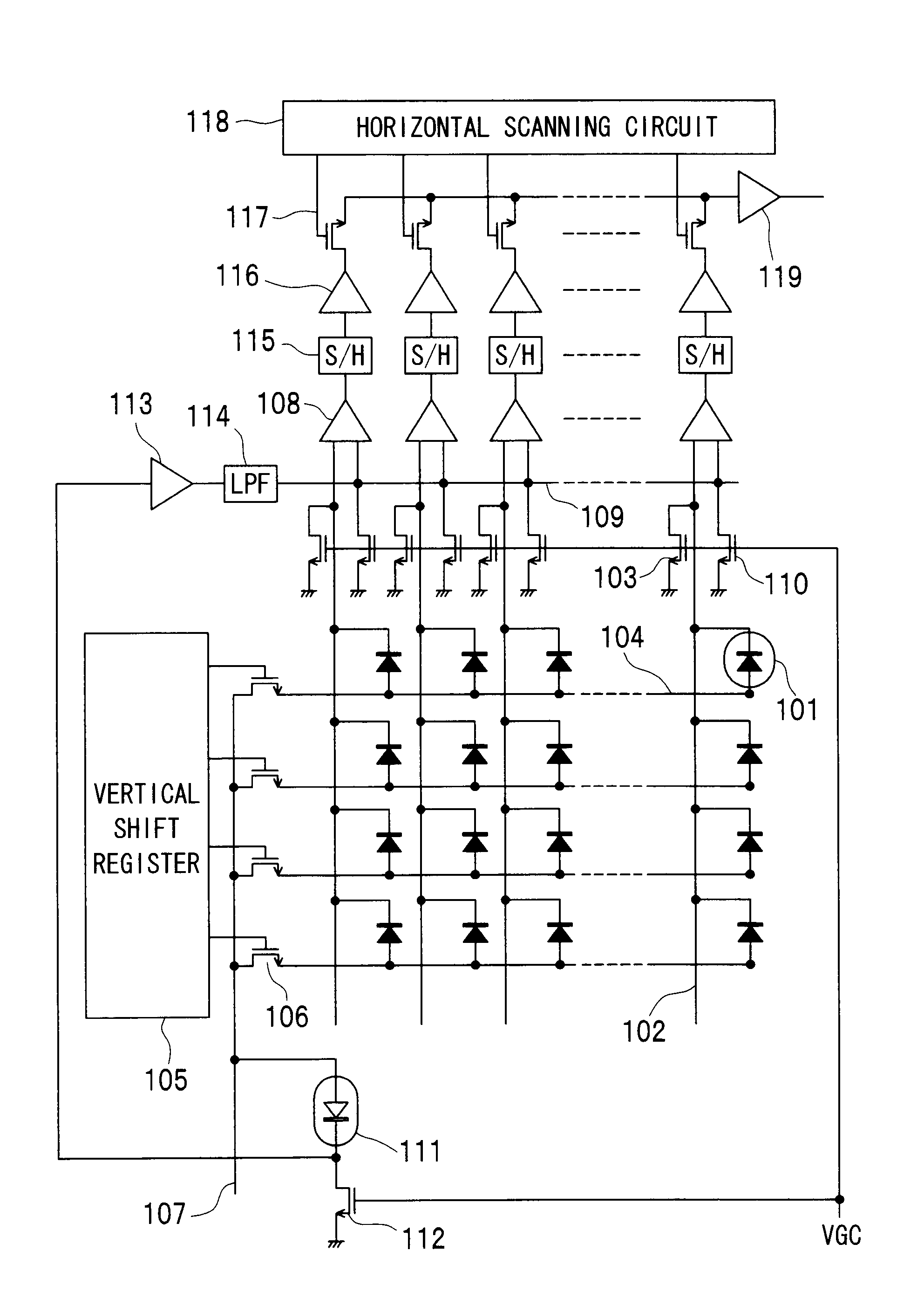
[0038]FIG. 1 is a circuit diagram of the thermal infrared solid state imaging device according to a first embodiment of the invention.

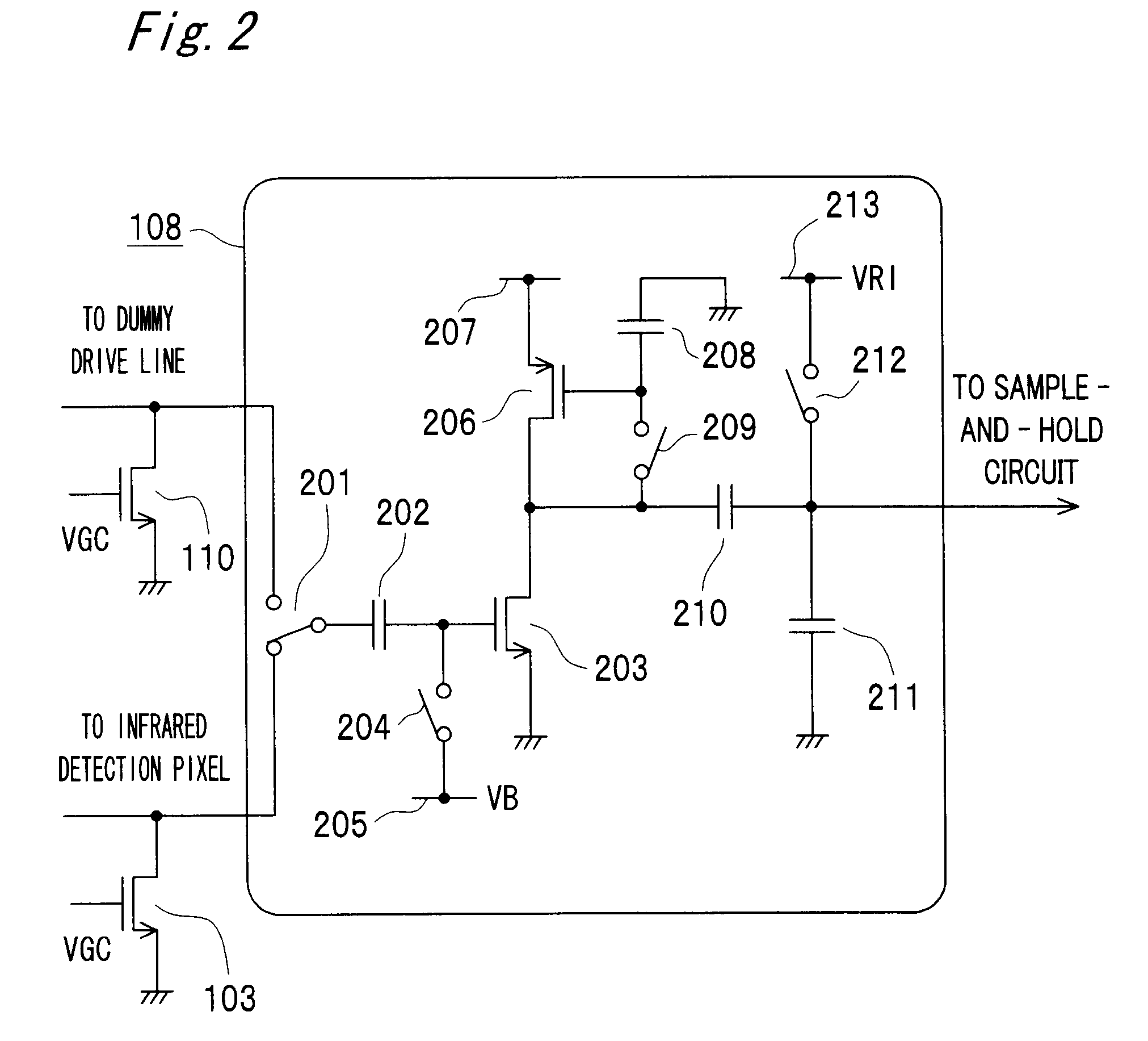
[0039]An infrared detection pixel 101 includes a heat-insulated diode. The infrared detection pixels 101 are arranged in a two-dimensional pixel matrix, forming a pixel area. The cathode of each infrared detection pixel 101 (diode) is connected in common by column to a vertical signal line 102, and a transistor 103 is connected to the end of each vertical signal line 102. The gates of the transistors 103 are connected in common, and a bias voltage VGC for operating in the saturation range is applied to the gates. The transistor 103 thus operates as a constant current source that supplies a constant current to the infrared detection pixel 101. The anodes of the infrared detection pixels 101 are connected in common by row by a horizontal signal line 104. The ends of the horizontal signal lines 1...

embodiment 2

[0074]FIG. 7 is a circuit diagram of a thermal infrared solid state imaging device according to a second embodiment of the invention. This embodiment applies the difference integration circuit described in the first embodiment to the infrared solid state imaging device taught in JP-A-2005-214639 which was previously filed by the applicant of the present application. The reference pixels 111 are disposed at the ends of the horizontal pixel lines in this embodiment of the invention.

[0075]A sample-and-hold circuit 701 samples the output of the reference pixel 111 that is output via the output amplifier 119. A bias generating circuit 702 compares the output from the sample-and-hold circuit 701 with a reference voltage Vref, outputs a decreasing voltage if the output of the reference pixel becomes greater than the reference voltage Vref, and outputs an increasing voltage if the reference pixel output becomes less than the reference voltage. The output voltage is applied through the low-p...

embodiment 3

[0078]FIG. 9 is a circuit diagram of a thermal infrared solid state imaging device according to a third embodiment of the invention. This embodiment applies the difference integration circuit described in the first embodiment to the infrared solid state imaging device taught in JP-A-2005-236717 which was previously filed by the applicant of the present application. In this embodiment, no reference pixel is used, and the entire pixel area is composed of infrared detection pixels 101.

[0079]FIGS. 10A and 10B are schematic diagrams of infrared cameras that use the infrared solid state imaging device according to the present embodiment.

[0080]The infrared camera shown in FIG. 10A has an infrared solid state imaging device 1004, a lens 1003, a pre-amplifier 1005, an A / D converter 1006, a digital signal processor (DSP) 1007, and D / A converter and amplifier circuit 1008. The lens 1003 focuses infrared light emitted by a subject on the infrared solid state imaging device 1004. The pre-amplifi...


PUM


Abstract

An infrared solid state imaging device includes a pixel area with arranged infrared detection pixels and a integration circuit for modulating output current based on the output of the pixel. The integration circuit contains an integrating transistor that modulates a current based on the difference in potential between first and second constant current devices, a integration capacitor for storing the modulated current and being reset periodically, a bias current supply transistor, a switch for connecting the drain with the gate of the bias current supply transistor, a capacitor providing AC coupling between the output of the integrating transistor and the integrating capacitor, a gate bias switch for providing the integrating transistor with a bias voltage, a switch for selecting, as input to the integrating transistor, either one of outputs from the first and second constant current devices, and a capacitor for providing AC coupling between the switch and the gate of the integrating transistor.

Description

BACKGROUND OF THE INVENTION[0001]1. Field of the Invention[0002]The present invention relates to a thermal infrared solid state imaging device that detects thermal variations from incident infrared light using a two-dimensional semiconductor sensor array, and relates more particularly to a thermal infrared solid state imaging device that outputs the result of integrating electrical signals from a semiconductor sensor by means of a signal processing circuit, and to an infrared camera that uses this thermal infrared solid state imaging device.[0003]2. Related Art[0004]Various technologies related to thermal infrared solid state imaging devices have been disclosed.[0005]For example, the thermal infrared solid state imaging device described in a non-patent document 1 (“A low cost 320×240 uncooled IRFPA using a conventional silicon IC process”, Ishikawa, et al., Part of the SPIE Conference on Infrared Technology and Applications XXV, April 1999, Vol. 3698, pp 556-564 (FIGS. 7 and 9)) has...

Claims


Application Information

Patent Timeline
Patent Type & Authority Patents(United States)
IPC IPC(8): G01J5/24
CPCG01J5/08H04N5/33G01J5/20G01J5/0853
Inventor UENO, MASASHI
Owner MITSUBISHI ELECTRIC CORP
Why Eureka
Try Eureka