Liquid crystal display device and method for manufacturing the same

a liquid crystal display and display device technology, applied in static indicating devices, instruments, non-linear optics, etc., can solve the problems of narrow viewing angle, insignificant view control effect, and difficulty in adjusting the viewing angle, so as to increase the viewing angle and reduce the viewing angle

Inactive Publication Date: 2010-06-01
LG DISPLAY CO LTD
View PDF10 Cites 15 Cited by
  • Summary
  • Abstract
  • Description
  • Claims
  • Application Information

AI Technical Summary

Benefits of technology

[0021]An advantage of the present invention is to provide a liquid crystal display device that can realize a narrow viewing angle in addition to a wide viewing angle in a fringe field switching (FFS) mode in such a way of allowing a white sub-pixel among RGBW-4 sub-pixels to be driven in the same FFS mode as that of the adjacent RGB sub-pixels for the wide viewing angle while being driven to form a vertical electric field different from that of the adjacent RGB sub-pixels only for the narrow viewing angle, and a method for manufacturing the same.
[0022]Additional advantages and features of the invention will be set forth in part in the description which follows and in part will become apparent from the descriptions or may be learned by practice of the invention. These and other advantages of the invention may be realized and attained by the structure particularly pointed out in the written description and claims hereof as well as the appended drawings.
[0023]To achieve these and other advantages and in accordance with the purpose of the invention, as embodied and broadly described herein, there is provided a liquid crystal display device, comprising: gate lines and data lines crossing each other to define RGBW sub-pixels on a first substrate; a thin film transistor formed at each crossing of the gate and data lines; a first common electrode formed in each region of the RGBW sub-pixels; a pixel electrode connected to the thin film transistor and insulated from the first common electrode, the pixel electrode having at least one slit attached to the first substrate, wherein the first and second substrates face each other with a liquid crystal layer interposed therebetween; and a second common electrode formed on the second substrate and corresponding to each W sub-pixel.
[0024]In accordance with another aspect of the present invention, there is provided a method for manufacturing a liquid crystal display device, comprising: forming first common electrodes on a first substrate; forming gate lines and data lines to cross each other to define RGBW sub-pixels on the first substrate; forming a thin film transistor at each crossing of the gate and data lines; forming a passivation layer on an overall surface of the first substrate including the thin film transistor; forming pixel electrodes on the passivation layer, each having at least one slit; attaching a second substrate to the first substrate, wherein the first substrate and second substrate face each other, the second substrate having a second common electrode formed to correspond only to each W sub-pixel; and forming a liquid crystal layer between the first and second substrates.
[0025]In this manner, the present invention is characterized in that the wide and narrow viewing angles are controlled by means of the white sub-pixel among the RGBS-4 sub-pixels, in which, with the second common electrode introduced only into each W sub-pixel on the second substrate (a color filter array substrate), a voltage is applied in such a way that, for the case of wide viewing angle, the second common electrode of the second substrate is supplied with the same level of voltage as that of the first common electrode of the first substrate (thin film transistor array substrate) or is not supplied with any voltage to make it in a floating state, and in the case of narrow viewing angle, an electric field difference of about 1˜4 V or about −4˜−1 V is induced between the second common electrode of the second substrate and the first common electrode of the first substrate.
[0026]That is, in the LCD device in which one pixel is constituted by RGBW four sub-pixels, the RGB sub-pixels are always driven in the FES mode, whereas the W sub-pixel is driven in the FFS mode for the wide viewing angle, thereby increasing a viewing angle, and generates the vertical electric field for the narrow viewing angle, thereby reducing the viewing angle.

Problems solved by technology

Although the TN type LCD device has been spotlighted in terms of its excellent contrast and color reproducibility, it suffers from a significant problem in that it has a narrow viewing angle.
Such a related art liquid crystal display device has problems as follows.
However, these techniques have some problems as follows.
First, the view control effect is insignificant.
Secondly, enlargement in the range of the electrode structure modified or added to increase the view control effect is very disadvantageous in view of an aperture ratio.
The most important problem of these techniques is in a complicated driving method due to insertion of the additional electrode layer and application of signals.

Method used


Image

  • Liquid crystal display device and method for manufacturing the same
  • Liquid crystal display device and method for manufacturing the same
  • Liquid crystal display device and method for manufacturing the same

Examples


Embodiment Construction

[0037]Reference will now be made in detail to embodiments of the present invention, examples of which are illustrated in the accompanying drawings. Wherever possible, the same reference numbers will be used throughout the drawings to refer to the same or like parts.

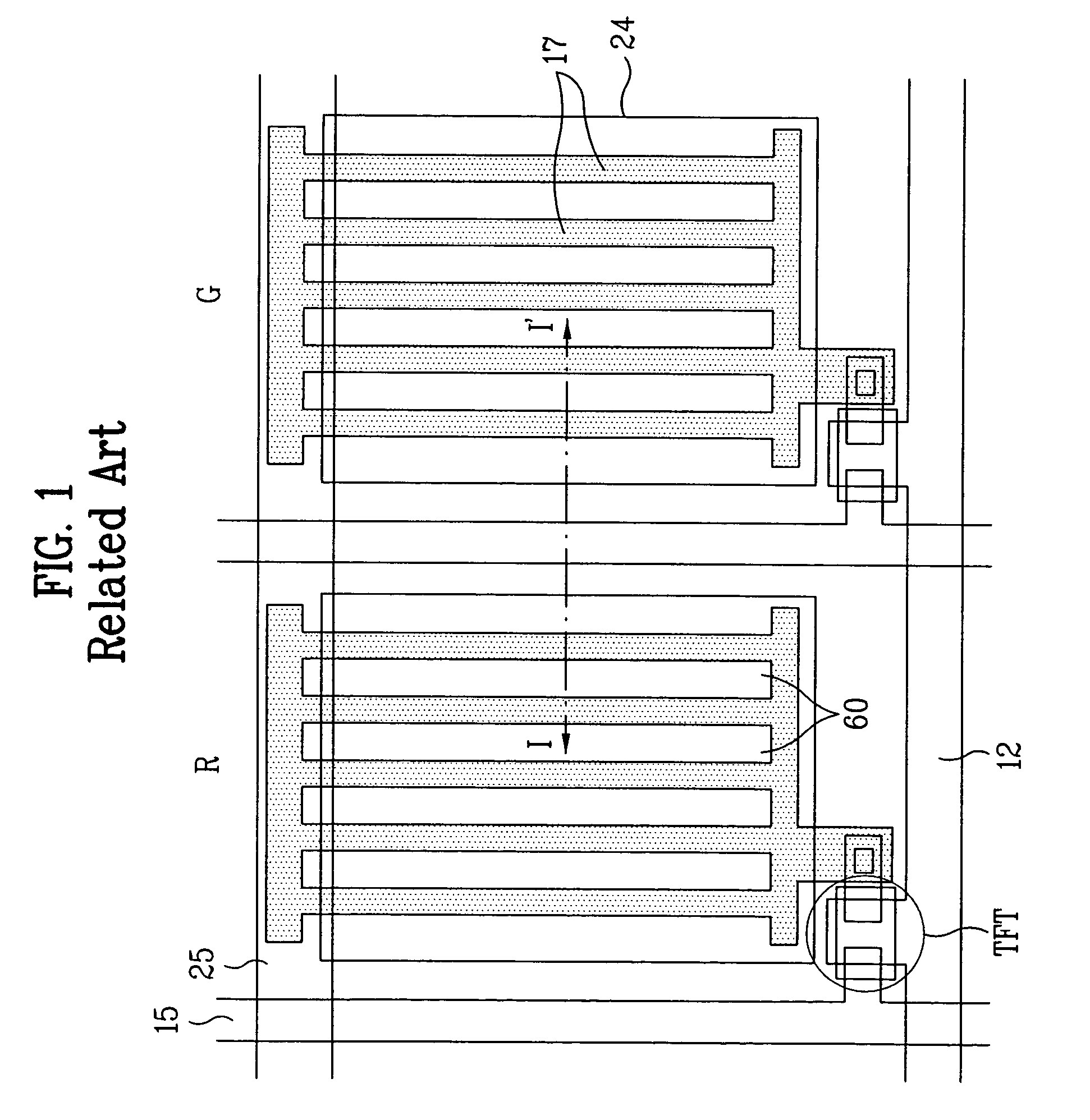
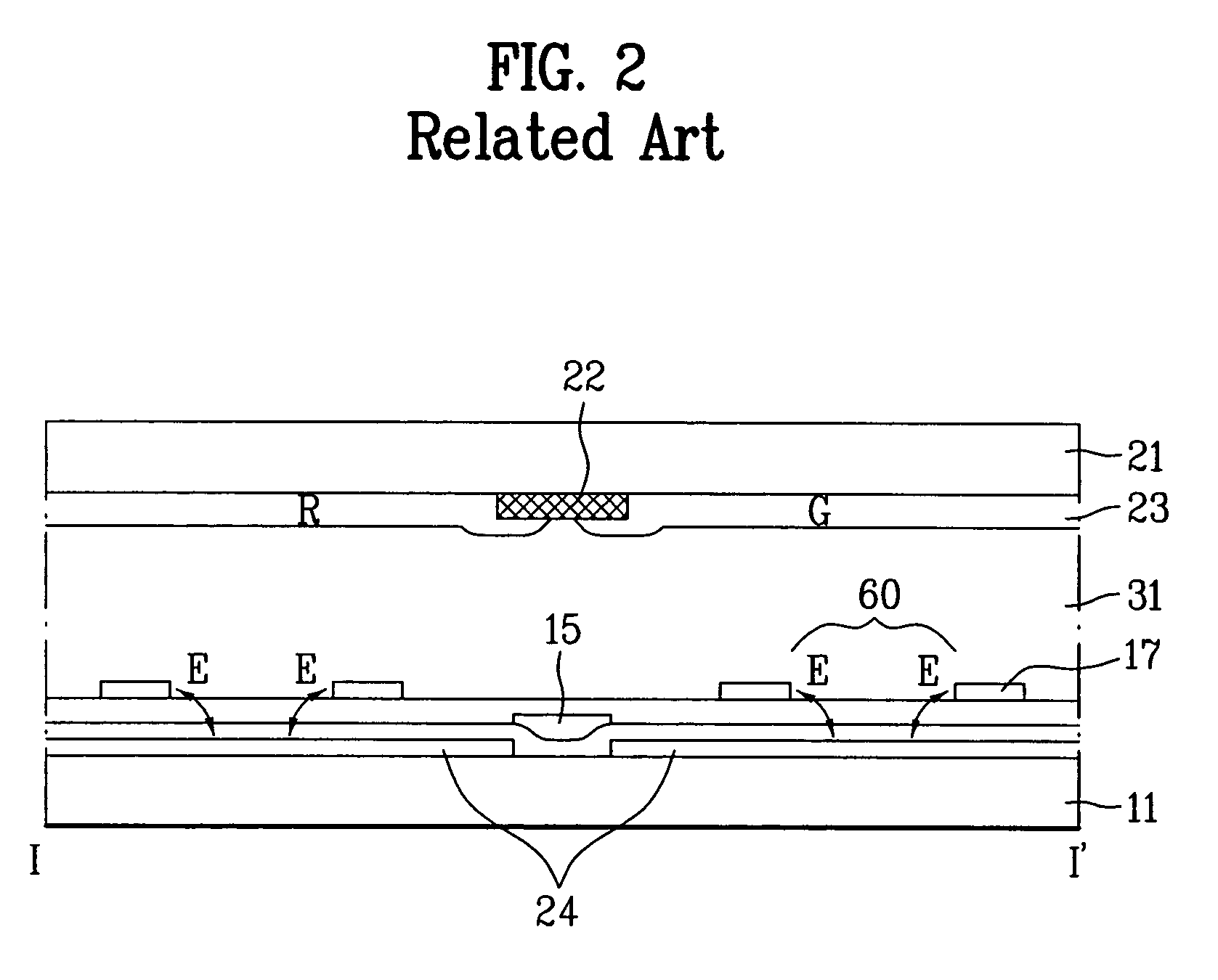
[0038]FIG. 3 is a plan view illustrating an FFS mode type LCD device according to the present invention, FIG. 4 is a cross-sectional view taken along line II-II′ of FIG. 3, and FIG. 5 is a view illustrating patterns on a color filter array substrate according to the present invention.

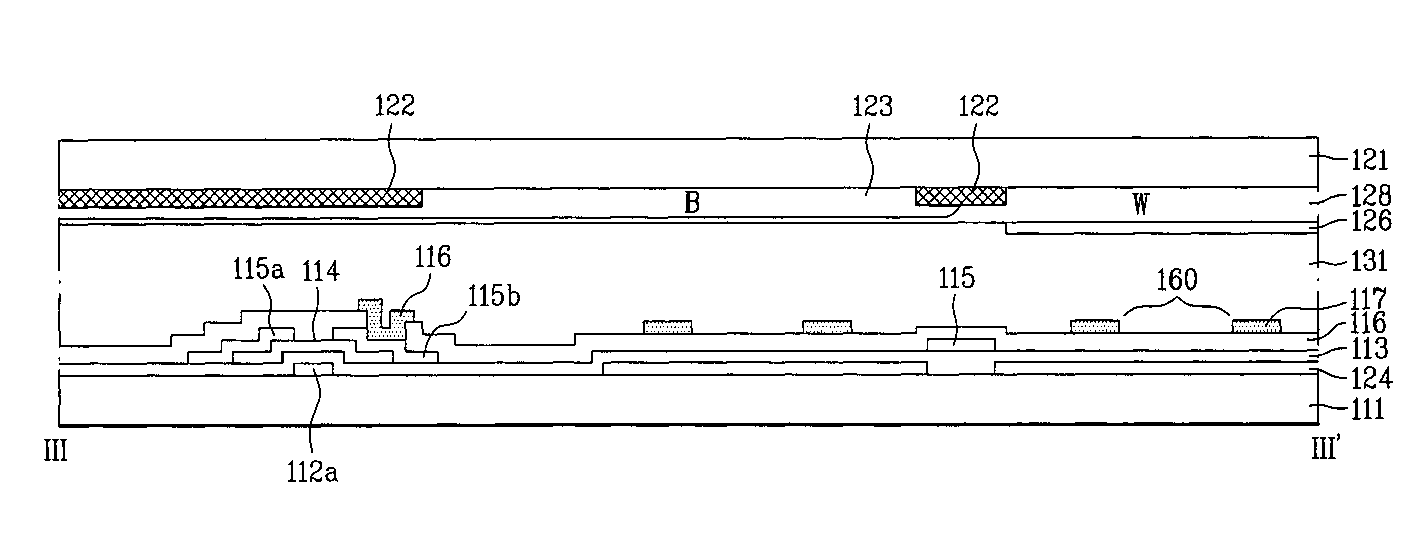
[0039]In addition, FIGS. 6A and 6B are cross-sectional views illustrating a mode for a wide viewing angle of the LCD device according to the present invention, FIGS. 7A and 7B are cross-sectional views illustrating a mode for a narrow viewing angle of the LCD device according to the present invention, and FIGS. 8A to 8D are cross-sectional views illustrating manufacturing steps taken along lines III-III′ of FIG. 3.

[0040]In FIGS. 3 and 4, the ...


PUM

PropertyMeasurementUnit
voltageaaaaaaaaaa
electric fieldaaaaaaaaaa
voltageaaaaaaaaaa

Abstract

A liquid crystal display device employs a white sub-pixel among RGBW-4 sub-pixels as a view control component to realize a narrow viewing angle or a wide viewing angle in a fringe field switching mode. The LCD device comprises gate lines and data lines crossing each other to define RGBW sub-pixels on a first substrate, a thin film transistor formed at each crossing of the gate and data lines; a first common electrode in each region of the RGBW sub-pixels, a pixel electrode connected to the thin film transistor and insulated from the first common electrode, the pixel electrode having at least one slit, a second substrate attached to the first substrate, wherein the first and second substrate face each other with a liquid crystal layer interposed therebetween, and a second common electrode on the second substrate and corresponding to each W sub-pixel.

Description

[0001]This application claims the benefit of Korean Patent Application No. 10-2005-0131564, filed on Dec. 28, 2005, which is hereby incorporated by reference as if fully set forth herein.BACKGROUND OF THE INVENTION[0002]1. Field of the Invention[0003]The present invention relates to a liquid crystal display (LCD) device, and a method for manufacturing the same. More particularly, the present invention relates to a liquid crystal display device that employs a white sub-pixel among RGBW-4 sub-pixels as a view control component to realize a narrow viewing angle as well as a wide viewing angle in a fringe field switching mode, and a method for manufacturing the same.[0004]2. Discussion of the Related Art[0005]In recent years, rapid advances in the performance of an active matrix liquid crystal display (“LCD”) device have resulted in various applications of the LCD device, such as screens for flat panel TVs, and monitors for portable computers.[0006]Among the active matrix LCD devices, a...

Claims


Application Information

Patent Timeline
Patent Type & Authority Patents(United States)
IPC IPC(8): G02F1/1335G02F1/1333
CPCG02F1/133514G02F1/134363G02F1/1362G09G3/3607G09G3/3648G02F1/1323G02F2201/52G09G2320/028G02F2001/134381G09G2300/0452G02F1/134381G02F1/1335G02F1/1343
Inventor JIN, HYUN SUKJANG, HYUNG SEOK
Owner LG DISPLAY CO LTD
Why Eureka
Try Eureka