Light emitting diode having side reflection layer

a light-emitting diode and side reflection technology, applied in the direction of semiconductor devices, semiconductor/solid-state device details, electrical apparatus, etc., can solve the problems of increasing light loss, achieve low deviation in electrical characteristics, easy adjustment of viewing angle, and good electrical reliability

Active Publication Date: 2020-06-25
SEOUL VIOSYS CO LTD
View PDF0 Cites 3 Cited by
  • Summary
  • Abstract
  • Description
  • Claims
  • Application Information

AI Technical Summary

Benefits of technology

[0006]Exemplary embodiments of the present disclosure provide a light emitting diode that has a narrow light viewing angle by reducing the amount of light emitted through a side surface thereof.
[0007]Exemplary embodiments of the present disclosure provide a light emitting diode that allows easy control of viewing angle.
[0008]Exemplary embodiments of the present disclosure provide a light emitting diode that can realize a narrow viewing angle while reducing deviation in electrical characteristics between light emitting diodes.
[0012]Exemplary embodiments of the present disclosure provide light emitting diodes that employ a side reflection layer and have a distance of 50 μm from an active layer to a light exit surface, thereby providing a viewing angle of 110 degrees or less. Furthermore, exemplary embodiments of the present disclosure provide light emitting diodes that exhibit good electrical reliability and low deviation in electrical characteristics therebetween by preventing short circuit while maintaining the distance between the side reflection layer and a metal layer.
[0013]Exemplary embodiments of the present disclosure provide light emitting diodes that employ a side reflection layer to have a narrow viewing angle by reducing the amount of light emitted through side surfaces thereof and can permit easy adjustment of the viewing angle through adjustment of a location of the side reflection layer. Furthermore, the side reflection layer is formed to be spaced apart from a first pad metal layer in the lateral direction to prevent electric connection between the side reflection layer and the pad metal layer, thereby securing good electrical stability.

Problems solved by technology

In addition, when a backlight light source module configured to spread light through a lens is used as in LED TVs, discharge of light emitted from a side surface of a light emitting diode through the lens is difficult, thereby causing increase in light loss.

Method used


Image

  • Light emitting diode having side reflection layer
  • Light emitting diode having side reflection layer
  • Light emitting diode having side reflection layer

Examples


Embodiment Construction

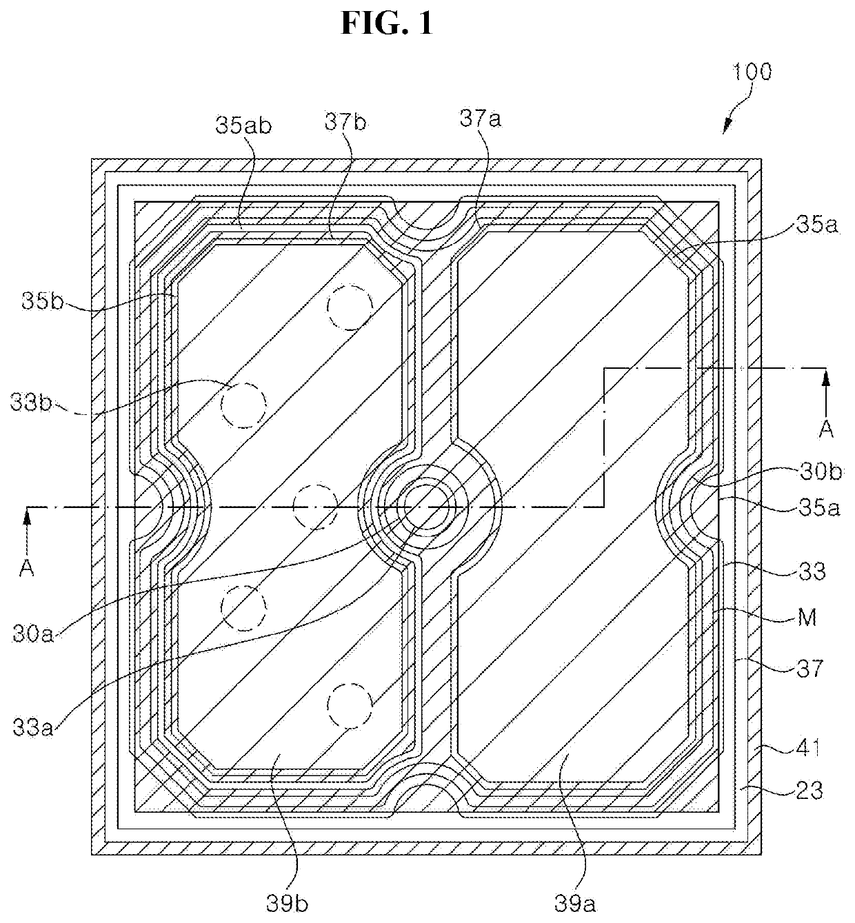
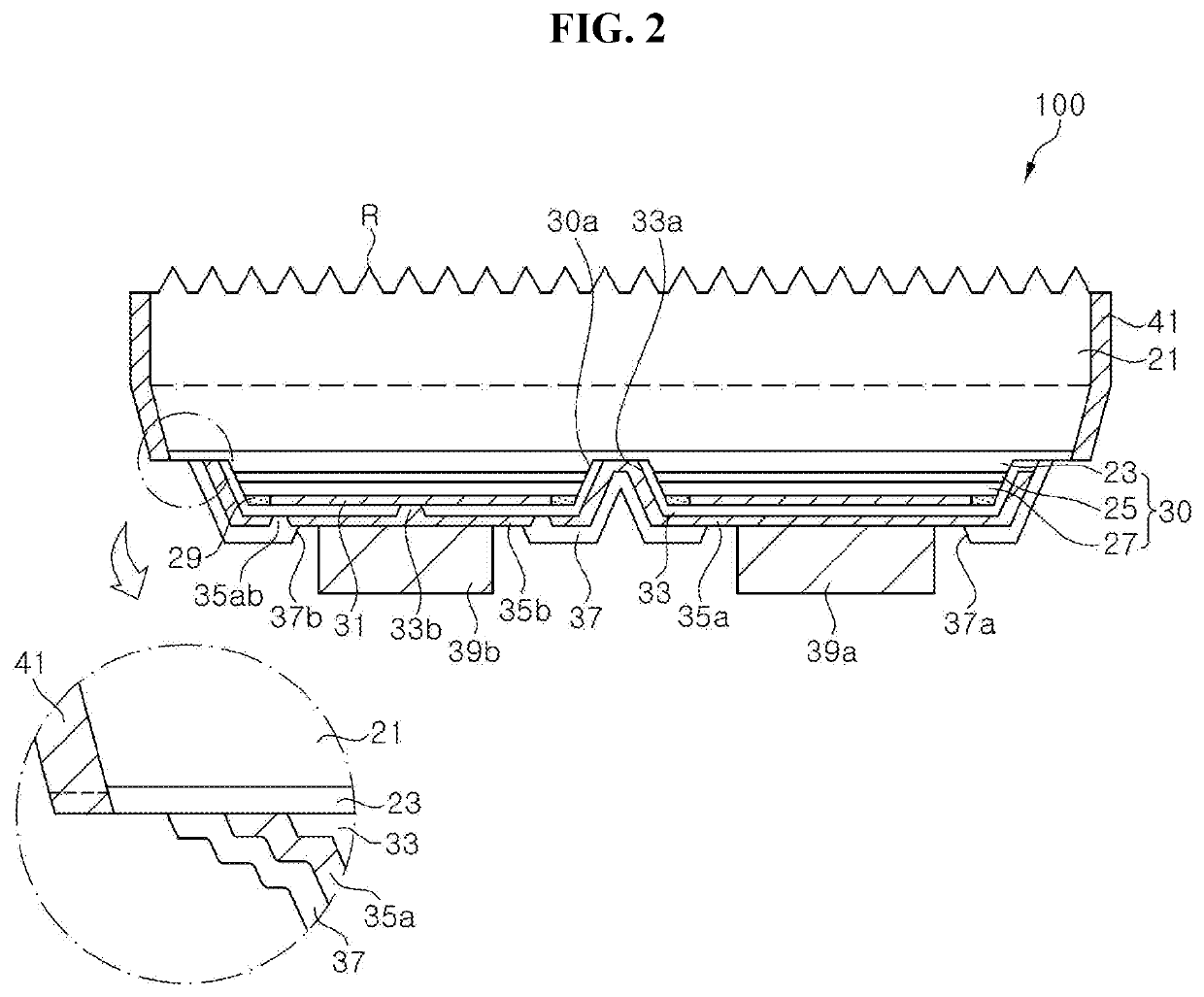
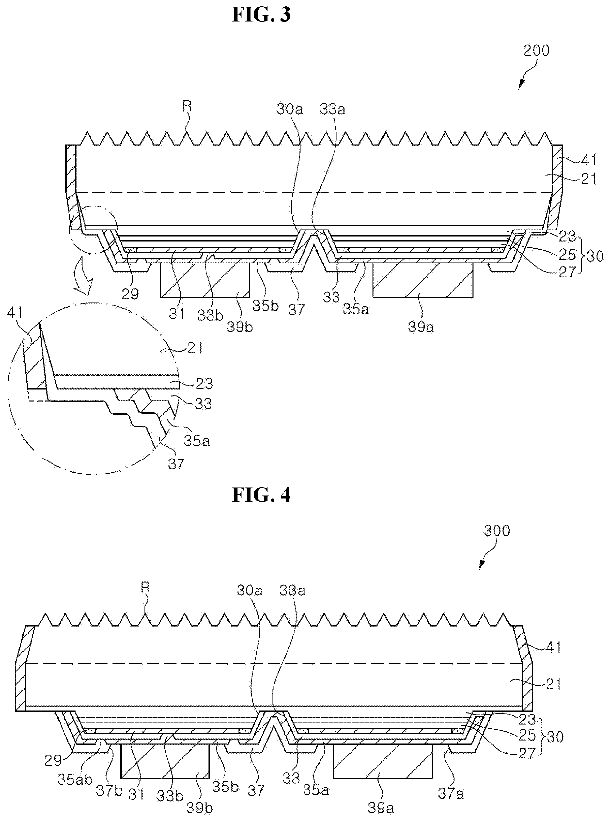
[0032]Hereinafter, exemplary embodiments of the present disclosure will be described in detail with reference to the accompanying drawings. The following embodiments are provided by way of example so as to fully convey the spirit of the present disclosure to those skilled in the art to which the present disclosure pertains. Accordingly, the present disclosure is not limited to the embodiments disclosed herein and can also be implemented in different forms. In the drawings, widths, lengths, thicknesses, and the like of elements can be exaggerated for clarity and descriptive purposes. When an element is referred to as being “disposed above” or “disposed on” another element, it can be directly “disposed above” or “disposed on” the other element, or intervening elements can be present. Throughout the specification, like reference numerals denote like elements having the same or similar functions.

[0033]In accordance with one exemplary embodiment of the present disclosure, a light emittin...


PUM

PropertyMeasurementUnit
distanceaaaaaaaaaa
inclination angleaaaaaaaaaa
light viewing angleaaaaaaaaaa

Abstract

A light emitting diode including a side reflection layer. The light emitting diode includes: a semiconductor stack and a light exit surface having a roughened surface through which light generated from an active layer is emitted; side surfaces defining the light exit surface; and a side reflection layer covering at least part of the side surfaces. The light exit surface is disposed over a first conductivity type semiconductor layer opposite to the ohmic reflection layer, all layers from the active layer to the light exit surface are formed of gallium nitride-based semiconductors, and a distance from the active layer to the light exit surface is 50 μm or more.

Description

CROSS-REFERENCE TO RELATED APPLICATION[0001]This application is a continuation of U.S. patent application Ser. No. 15 / 811,900, filed on Nov. 14, 2017, and claims priority from and the benefit of U.S. Provisional Application Nos. 62 / 422,015, filed on Nov. 14, 2016, and 62 / 461,405, filed on Jan. 21, 2017, all of which are incorporated by reference for all purposes as if fully set forth herein.BACKGROUNDField[0002]Exemplary embodiments of the present disclosure relate to a light emitting diode and, more particularly, a light emitting diode including a side reflection layer to adjust a viewing angle.Discussion of the Background[0003]Recently, with good thermal stability and a direct transition type energy band structure, Group III-based nitrides such as gallium nitride (GaN), aluminum nitride (AlN), and the like have been spotlighted as materials for light sources in the visible range and the ultraviolet range. Particularly, blue and green light emitting diodes using indium gallium nitr...

Claims


Application Information

Patent Timeline
Patent Type & Authority Applications(United States)
IPC IPC(8): H01L33/10H01L33/60H01L23/00
CPCH01L33/10H01L33/60H01L24/13H01L33/20H01L33/405H01L33/46H01L33/007H01L2933/0016H01L33/22H01L33/0093H01L33/32H01L2933/0025
Inventor JANG, JONG MINKIM, CHAE HONKIM, CHANG YOUNLIM, JAE HEE
Owner SEOUL VIOSYS CO LTD
Why Eureka
Try Eureka