Light emitting diode

a technology of light-emitting diodes and diodes, which is applied in the direction of semiconductor devices, semiconductor/solid-state device details, electrical apparatus, etc., can solve the problems of limiting the application of light-emitting chips, affecting the popularity of conventional light-emitting diodes, and increasing manufacturing costs

Active Publication Date: 2010-06-22
LITE ON TECH CORP
View PDF6 Cites 1 Cited by
  • Summary
  • Abstract
  • Description
  • Claims
  • Application Information

AI Technical Summary

Benefits of technology

[0008]Therefore, the object of the present invention is to provide a light emitting diode that can avoid color deviation of light obtained therefrom.

Problems solved by technology

However, these methods can only be applied to the light emitting chip 12 that is mounted to the base 11 via chip bonding process (see FIG. 4) rather than wire bonding process.
Furthermore, these methods lead to higher manufacturing costs, thereby impeding the popularity of the conventional light emitting diode.

Method used


Image

  • Light emitting diode
  • Light emitting diode
  • Light emitting diode

Examples


Embodiment Construction

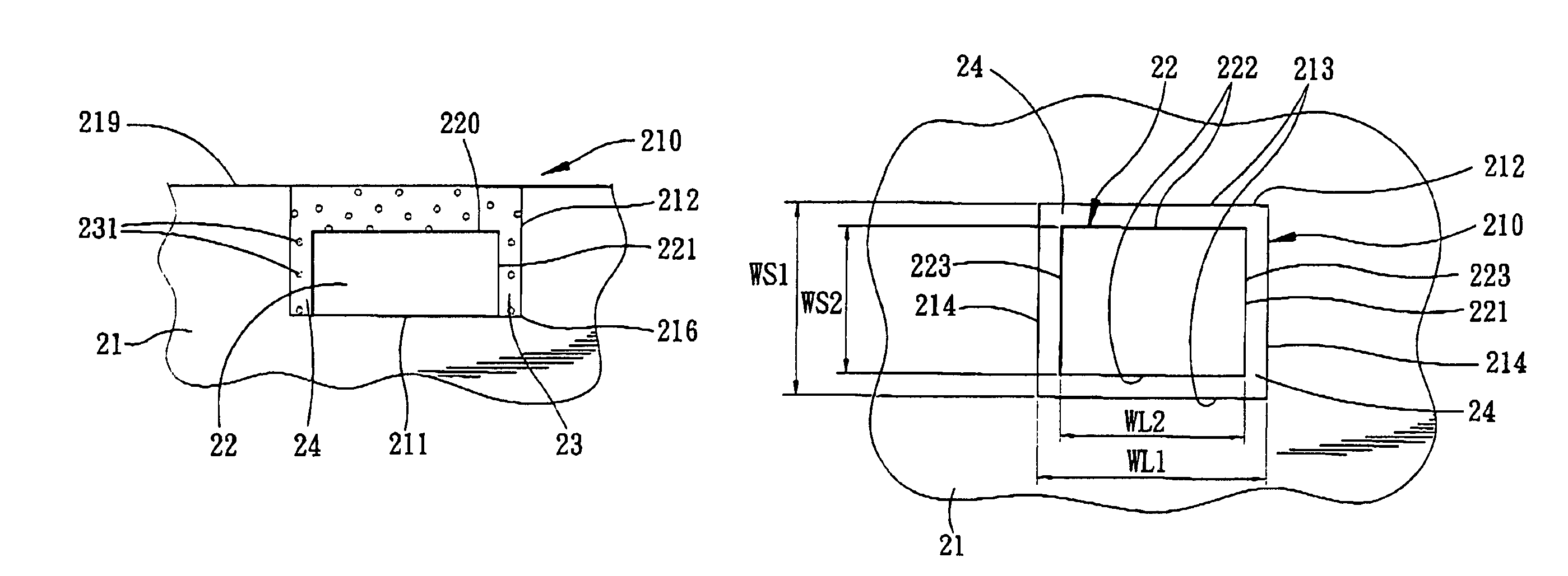
[0019]As shown in FIGS. 5 and 6, the preferred embodiment of a light emitting diode according to the present invention comprises a base 21, a light emitting chip 22, and a wavelength converting layer 23.

[0020]The base 21 has a top surface 219, and is formed with a recessed portion 210 that is indented from the top surface 219. The recessed portion 210 has a bottom wall surface 211 having a periphery 216, and a side wall surface 212 extending upwardly from the periphery 216 of the bottom wall surface 211 to the top surface 219 of the base 21 and cooperating with the bottom wall surface 211 to define a receiving space 215.

[0021]The light emitting chip 22 is provided in the receiving space 215 and is disposed on the bottom wall surface 211 of the recessed portion 210 such that a geometric center of the light emitting chip 12 coincides with that of the bottom wall surface 211 of the recessed portion 210. The light emitting chip 22 has a top chip surface 220 that is disposed below the to...


PUM


Abstract

A light emitting diode includes a base, a light emitting chip, and a wavelength converting layer. The base is formed with a recessed portion that has a bottom wall surface, and a side wall surface extending upwardly from the bottom wall surface and cooperating with the bottom wall surface to define a receiving space. The light emitting chip is provided on the bottom wall surface of the receiving space, and has a top chip surface disposed below a top surface of the base, and a peripheral chip surface extending downwardly from the top chip surface and being substantially parallel to and forming a gap with the side wall surface of the recessed portion. The wavelength converting layer is filled in the receiving space in the recessed portion so as to cover the top chip surface and the peripheral chip surface of the light emitting chip.

Description

CROSS-REFERENCE TO RELATED APPLICATION[0001]This application claims priority of Taiwanese Application No. 096115904, filed on May 4, 2007.BACKGROUND OF THE INVENTION[0002]1. Field of the Invention[0003]The invention relates to a light emitting device, more particularly to a light emitting diode.[0004]2. Description of the Related Art[0005]As shown in FIG. 1, a conventional light emitting diode includes a base 11 formed with a recessed portion 111, a light emitting chip 12 provided on a bottom wall surface of the recessed portion 111 and having a top chip surface and a peripheral chip surface, and a fluorescent layer 13 filled in the recessed portion 111 so as to cover the top chip surface and the peripheral chip surface of the light emitting chip 12. The fluorescent layer 13 contains phosphor particles 131 for converting a part of blue light emitted from the light emitting chip 12 into yellow light, so that the mix of blue and yellow light results in white light. However, since ligh...

Claims


Application Information

Patent Timeline
Patent Type & Authority Patents(United States)
IPC IPC(8): H01L33/00H01L21/00H01L33/50H01L33/60
CPCH01L33/505H01L33/60H01L2924/0002H01L2924/00
Inventor WU, CHIA-HAOLEE, TIEN-YU
Owner LITE ON TECH CORP
Why Eureka
Try Eureka