Metal-metal bonding of compliant interconnect

a technology of metal-metal bonding and compliant interconnect, which is applied in the direction of semiconductor/solid-state device details, electrical devices, semiconductor devices, etc., and can solve problems such as harm

Active Publication Date: 2010-07-06
INTEL CORP
View PDF39 Cites 43 Cited by
  • Summary
  • Abstract
  • Description
  • Claims
  • Application Information

AI Technical Summary

Problems solved by technology

Further, solders typically used in part to form the interconnects between the components can cause harmful effects and may be, in some cases, unlawful to use in the near future.

Method used


Image

  • Metal-metal bonding of compliant interconnect
  • Metal-metal bonding of compliant interconnect
  • Metal-metal bonding of compliant interconnect

Examples


Embodiment Construction

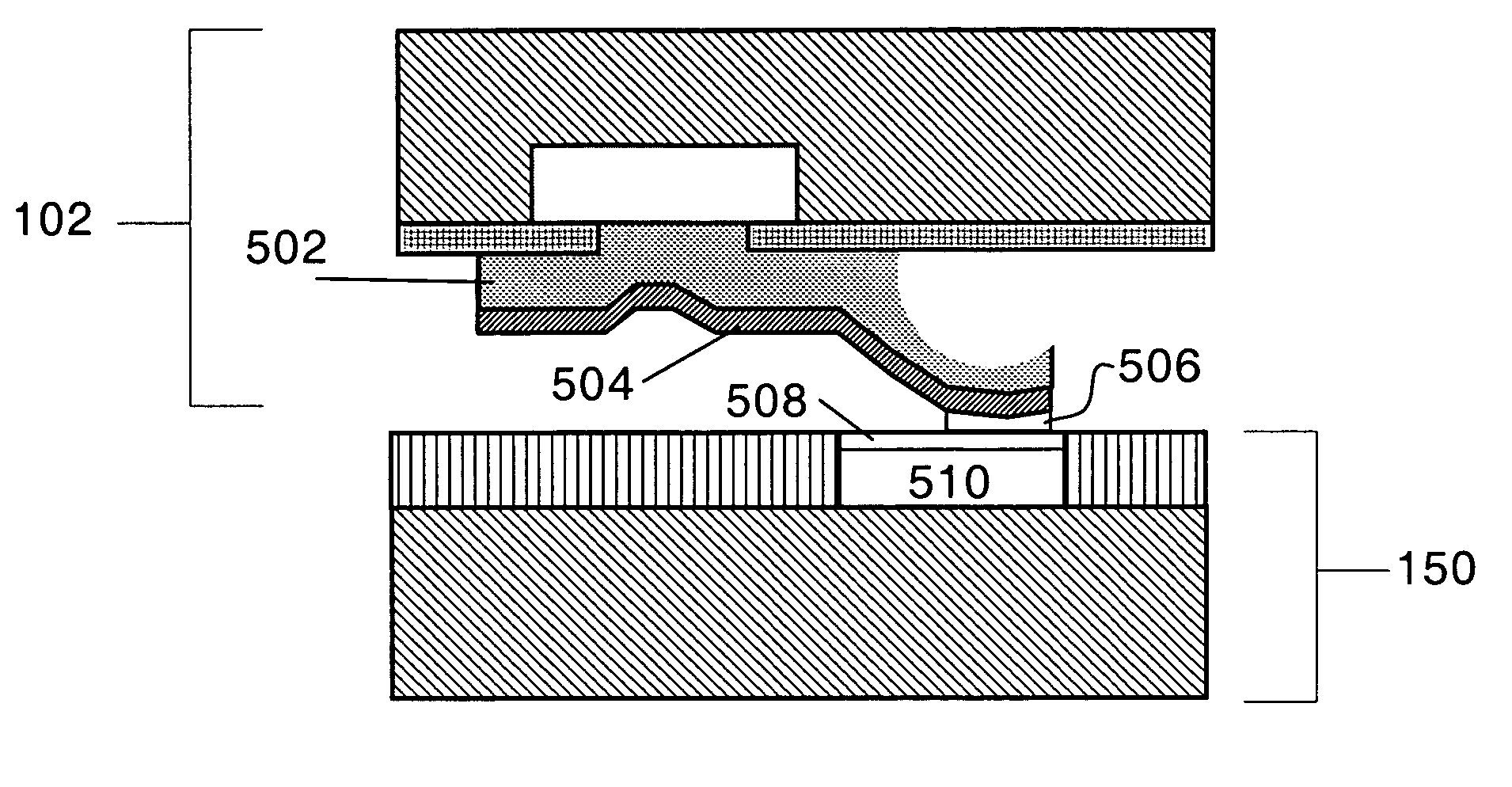
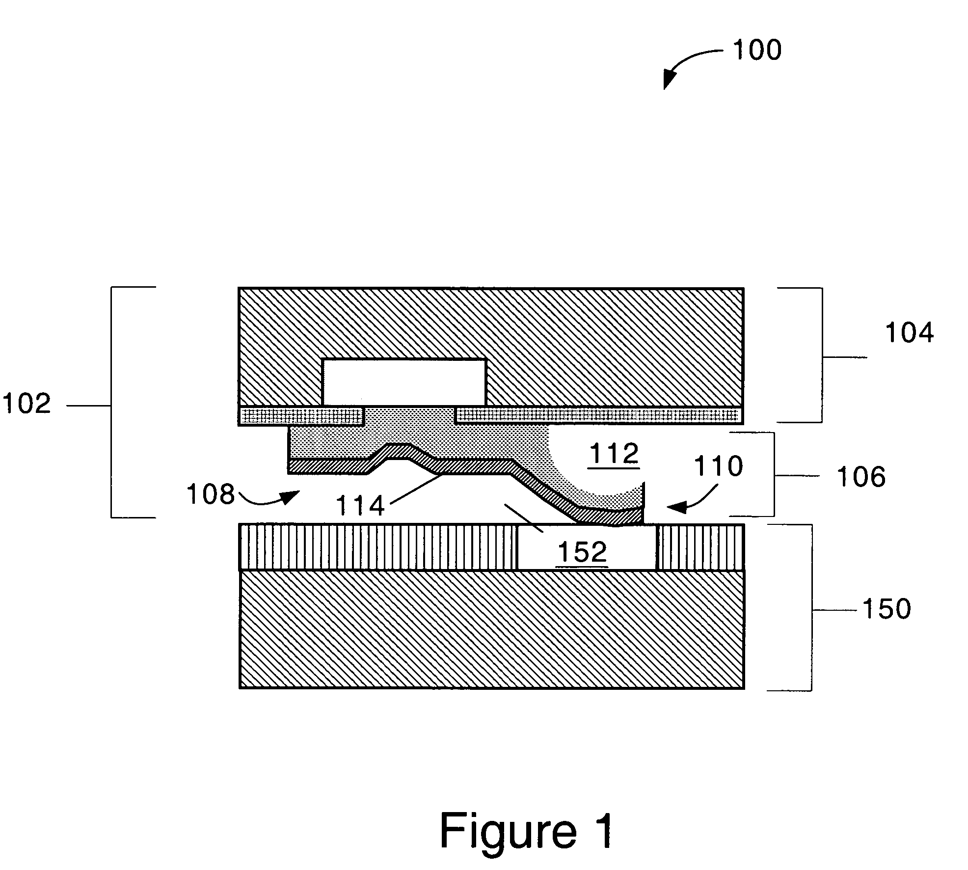
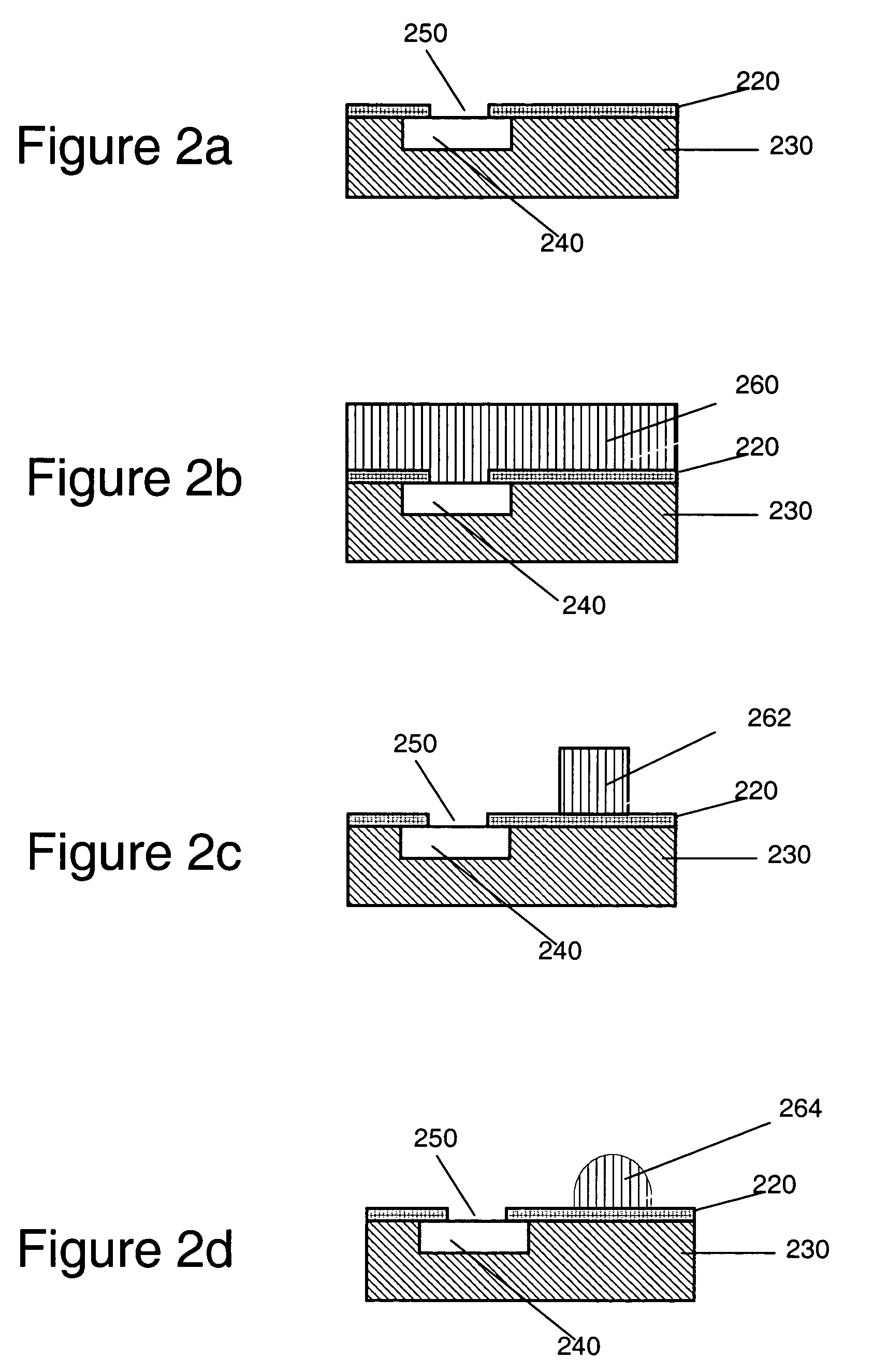
[0009]FIG. 1 is a side cross sectional view of a bonded apparatus 100 according to one embodiment of the invention. The apparatus 100 includes a microelectronic die 102, such as a microprocessor die 102. In some embodiments, a device other than a microelectronic die 102 may used instead of the die. For the purposes of the description of one embodiment below, the die 102 will be described as a microprocessor die 102, although it may be other devices in other embodiments.

[0010]The die 102 may include a die substrate 104. The die substrate 104 may include one or more layers and devices. The substrate 104 may include conducting material, insulating material, semiconducting material, and other materials or material combinations. For example, in an embodiment where the device 102 is a microprocessor die, the substrate 104 may include many millions of transistors.

[0011]The die 102 may also include a compliant interconnect 106. The compliant interconnect 106 may be electrically connected to...


PUM

PropertyMeasurementUnit
thickaaaaaaaaaa
thickaaaaaaaaaa
thickaaaaaaaaaa

Abstract

Embodiments of the invention provide a first component with a compliant interconnect bonded to a second component with a land pad by a metal to metal bond. In some embodiments, the first component may be a microprocessor die and the second component a package substrate.

Description

BACKGROUNDBackground of the Invention[0001]To make an integrated circuit device, such as microprocessors or other related computer components, a microelectronic die is often bonded to another component, such as a package substrate. Interconnects between the die and the package substrate transmit electrical signals between the two components. For performance and other reasons, modern semiconductor packages and MEMS (micro electromechanical systems) often employ ultra low k (dielectric value) interlayer dielectric layers, which typically have low mechanical strength. Accordingly, the interlayer dielectric layers are more sensitive to stress. Further, solders typically used in part to form the interconnects between the components can cause harmful effects and may be, in some cases, unlawful to use in the near future.BRIEF DESCRIPTION OF THE DRAWINGS[0002]FIG. 1 is a side cross sectional view of a bonded apparatus according to one embodiment of the invention.[0003]FIGS. 2a through 2h ar...

Claims


Application Information

Patent Timeline
Patent Type & Authority Patents(United States)
IPC IPC(8): H01L23/48
CPCH01L24/10H01L24/13H01L2224/13099H01L2924/1461H01L2924/014H01L2924/01013H01L2924/01022H01L2924/01027H01L2924/01029H01L2924/01042H01L2924/01046H01L2924/01073H01L2924/01077H01L2924/01078H01L2924/01079H01L2924/01082H01L2924/14H01L2924/01006H01L2924/01019H01L2924/01024H01L2924/01033H01L2924/01044H01L2924/01045H01L2924/01047H01L2924/01076H01L2924/00H01L2224/13H01L2224/05022H01L2224/05548H01L2224/05001H01L2224/05611H01L2224/05624H01L2224/05639H01L2224/05644H01L2224/05647H01L2224/05655H01L2224/05666H01L2224/05669H01L2224/05671H01L2224/05681H01L2924/00014H01L24/05H01L2224/05099
Inventor MUTHUKUMAR, SRIRAMRAMANATHAN, SHRIRAM
Owner INTEL CORP
Why Eureka
Try Eureka