
Semiconductor integrated circuit

a technology of integrated circuits and semiconductors, applied in the field of semiconductor integrated circuits, can solve the problems of excessive power consumption, heat degrade the performance of the circuit, circuit limits the number of transistors that can be combined, etc., and achieve the effect of improving the error occurrence of estimation, performance drop or leakage current increas

Inactive Publication Date: 2010-07-06
SAMSUNG ELECTRONICS CO LTD
View PDF18 Cites 4 Cited by
  • Summary
  • Abstract
  • Description
  • Claims
  • Application Information

AI Technical Summary

Benefits of technology

[0032]Accordingly, exemplary embodiments of the present invention provide a semiconductor integrated circuit, and a method of fabricating the same, that is capable of improving error occurrence in estimation for a size, number and structure of an NMOS transistor or PMOS transistor in a semiconductor integrated circuit having a power gate or MTCMOS. Further, a product development or production impossibility based on a performance drop or leakage current increase or a yield decrease, in the semiconductor integrated circuit having a power gate or MTCMOS may be improved. Furthermore, in performing a revision when an error in the estimation for the size, number and structure etc. of NMOS transistor or PMOS transistor is generated, the difficulty of a product development being delayed by a mask revision that is required form a transistor level, may be improved.

Problems solved by technology

But excessive power consumption in the circuit limits the number of transistors that can be combined.
The excessive power consumption increases a generation of heat in the circuit, and the heat degrades the performance of the circuit, as well as the system employing the circuit.
Further, excessive power consumption may shorten a change period of secondary batteries in portable instruments that use the secondary batteries as the main power supply source.
In general, the main causes of power consumption in a MOS circuit may be based on a switching power and a short-circuit current, as well as being based on a leakage current and the like.
More specifically, the power consumption based on the leakage current occurs by a leakage current generated in a stop mode.
In order to meet such requirement it is difficult to find an appropriate method except a revision of the circuit design.
If the revision is not performed, the semiconductor integrated circuit may face a performance drop or leakage current increase.
That is, in case a pre-computed or simulated leakage current value actually has an error in a semiconductor integrated circuit on a wafer, the revision should be performed, or a product development or production impossibility due to a performance drop or leakage current increase should be accepted without any other solution, further bringing about a yield decrease or performance drop.
Even though the revision is performed, a mask revision is needed from a transistor level, so that the product development may be delayed.
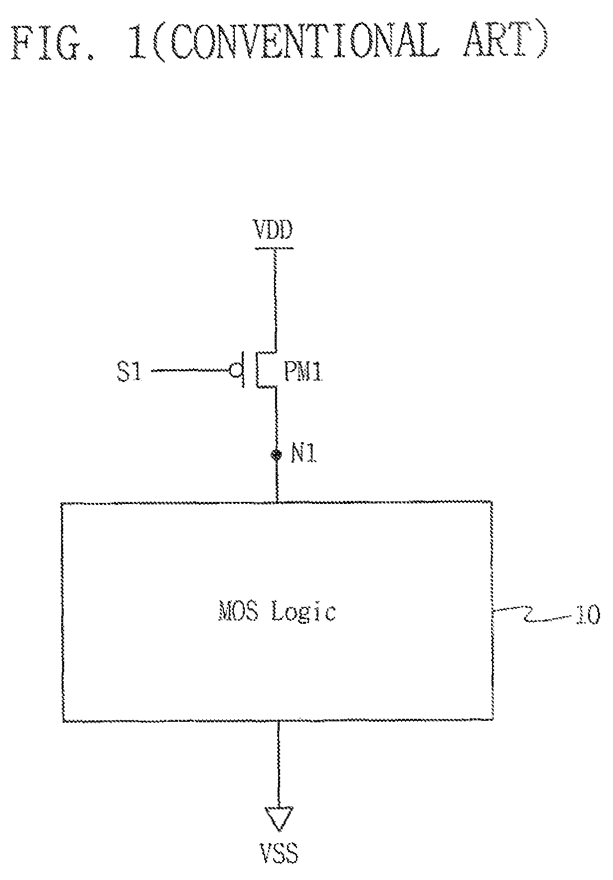
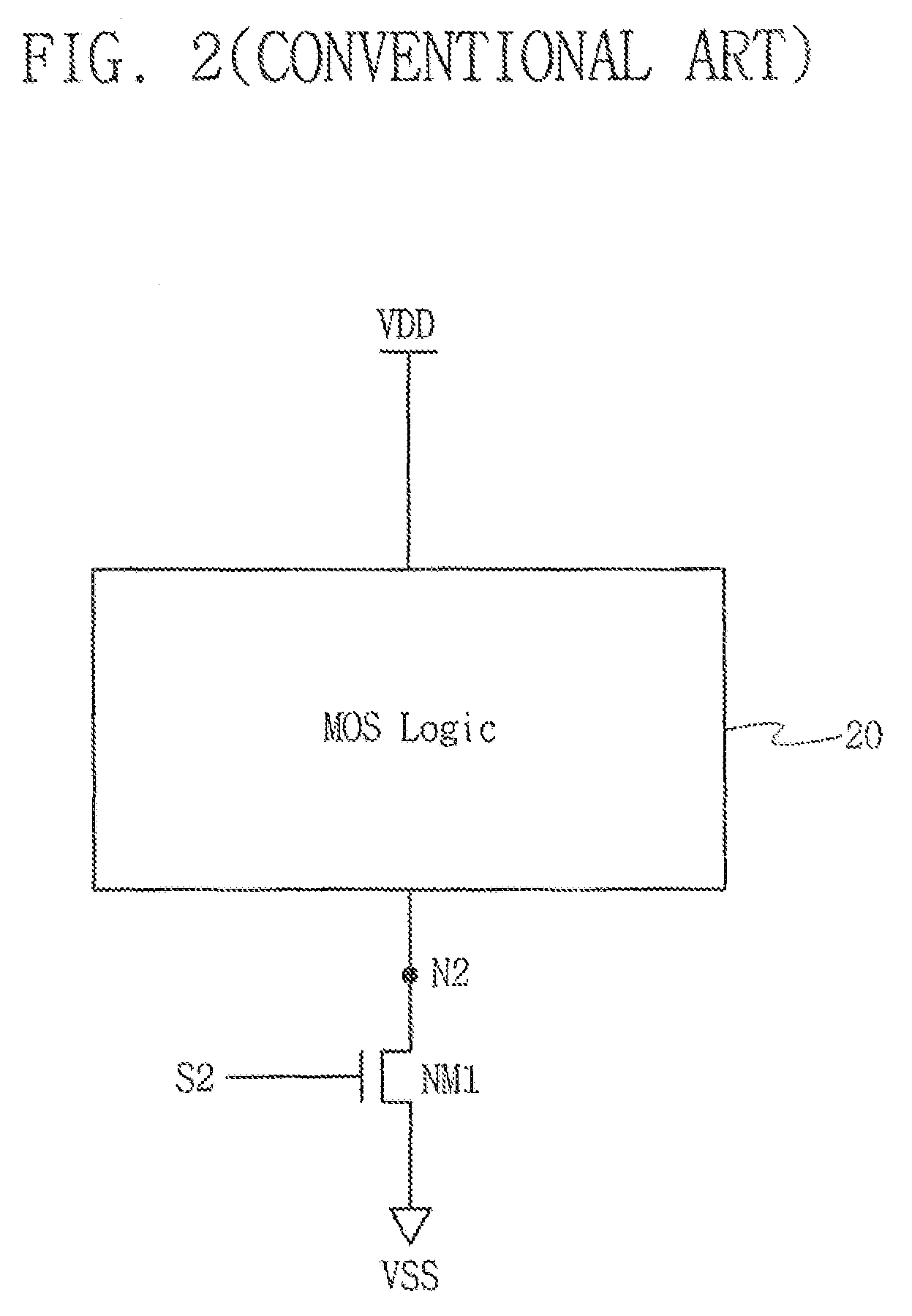
Similar problems may occur in the MTCMOS structure of FIG. 2 just as in in the power gate structure shown in FIG. 1, such as a dependency upon a circuit revision, or a product development or production impossibility based on a performance drop or leakage current increase, or a yield decrease or performance drop.
This approach, however, also has problems similar to those in the power gate structure and the MTCMOS structure shown in FIGS. 1 and 2.
For example, such problems involve a dependency upon the circuit revision, or a product development or production impossibility based on a performance drop or leakage current increase, or a shield decrease.
Also, a mask revision is required from a transistor level, thereby delaying a development schedule.

Method used


Image

  • Semiconductor integrated circuit
  • Semiconductor integrated circuit
  • Semiconductor integrated circuit

Examples


Embodiment Construction

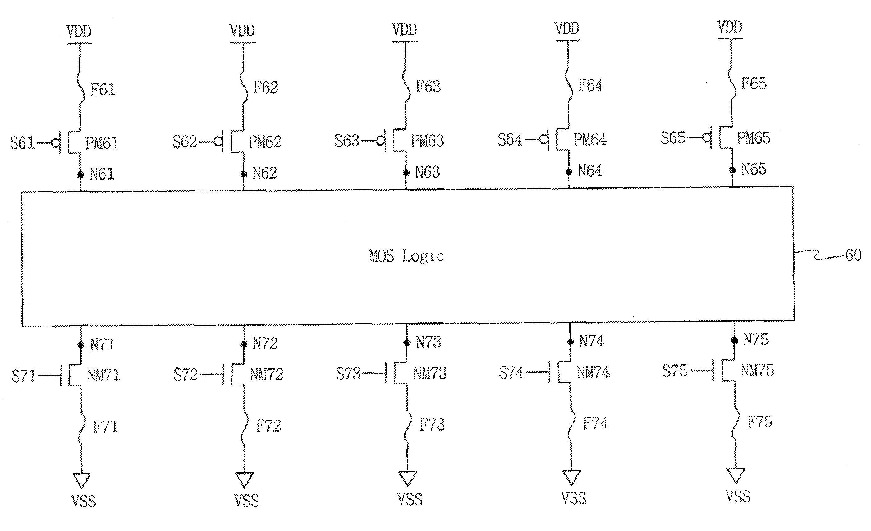
[0059]Exemplary embodiments of the present invention now will be described more fully hereinafter with reference to the accompanying drawings. This invention may, however, be embodied in many different forms and should not be construed as limited to the exemplary embodiments set forth herein. Rather these exemplary embodiments are provided so that this disclosure will be thorough and complete, and will fully convey the scope of the invention to those skilled in the art. Exemplary embodiments of the present invention are more fully described below with reference to FIGS. 4 to 8. This invention may, however, be embodied in many different forms and should not be construed as being limited to the exemplary embodiments set forth herein; rather, these exemplary embodiments are provided so that this disclosure is thorough and complete, and conveys the concept of the invention to those skilled in the art.

[0060]FIG. 4 is a circuit diagram illustrating an example of a semiconductor integrated...


PUM


Abstract

A semiconductor integrated circuit includes a MOS logic operating by first and second voltages; a switching transistor unit disposed between a supply terminal of the first voltage or the second voltage and the MOS logic, and turned on or off in response to a control signal so as to control a supply of the first or second voltage to the MOS logic; and a fuse unit disposed between the supply terminal of the first voltage or the second voltage and the switching transistor unit, for cutting off a supply of the first or second voltage to the switching transistor unit by a selective cut based on a test result. Whereby, a product development or production difficulty or a yield decrease based on a performance drop or leakage current increase in a circuit having a power gate or MTCMOS may be improved. In addition, a product development delay caused by a mask revision required at a transistor level may be improved in a revision of an NMOS or PMOS transistor.

Description

CROSS REFERENCE TO RELATED APPLICATION[0001]This application claims priority under 35 U.S.C. §119 from Korean Patent Application 10-2006-0067937, filed on Jul. 20, 2006, the contents of which are hereby incorporated by reference in their entirety herein.BACKGROUND OF THE INVENTION[0002]1. Technical Field[0003]The present disclosure relates to semiconductor circuits, and more particularly, to a semiconductor integrated circuit including a power gate or a multi-threshold CMOS device (MTCMOS) and a method of fabricating the same, in order to reduce a leakage current in a stop mode.[0004]2. Discussion of Related Art[0005]At present, performance of VLSI (Very Large Scale Integration) circuits and a combination capability of realizing respective circuits in one chip have been undergoing remarkable development. In particular, the increased number of image systems and radio communication equipment and the like requires circuits capable of performing various complicated functions. In order t...

Claims


Application Information

Patent Timeline
Patent Type & Authority Patents(United States)
IPC IPC(8): H03K17/16H03K19/003
CPCH03K19/0013H03K19/0016H01L27/02H01L21/82H01L27/06
Inventor JUNG, JIN-KOOK
Owner SAMSUNG ELECTRONICS CO LTD
Learn More