

Printed circuit board unit and electronic apparatus
a printed circuit board and electronic device technology, applied in the direction of laminating printed circuit boards, laminating device connections, semiconductor/solid-state device details, etc., can solve the problems of failure of electric conduction between the first electrically-conductive terminal/terminal and the corresponding second, and achieve the effect of enhancing the rigidity of the second board, reducing the thickness of the first board, and ensuring the effect of electrical conduction
- Summary
- Abstract
- Description
- Claims
- Application Information
AI Technical Summary
Benefits of technology
Problems solved by technology
Method used
Image

Examples
Embodiment Construction
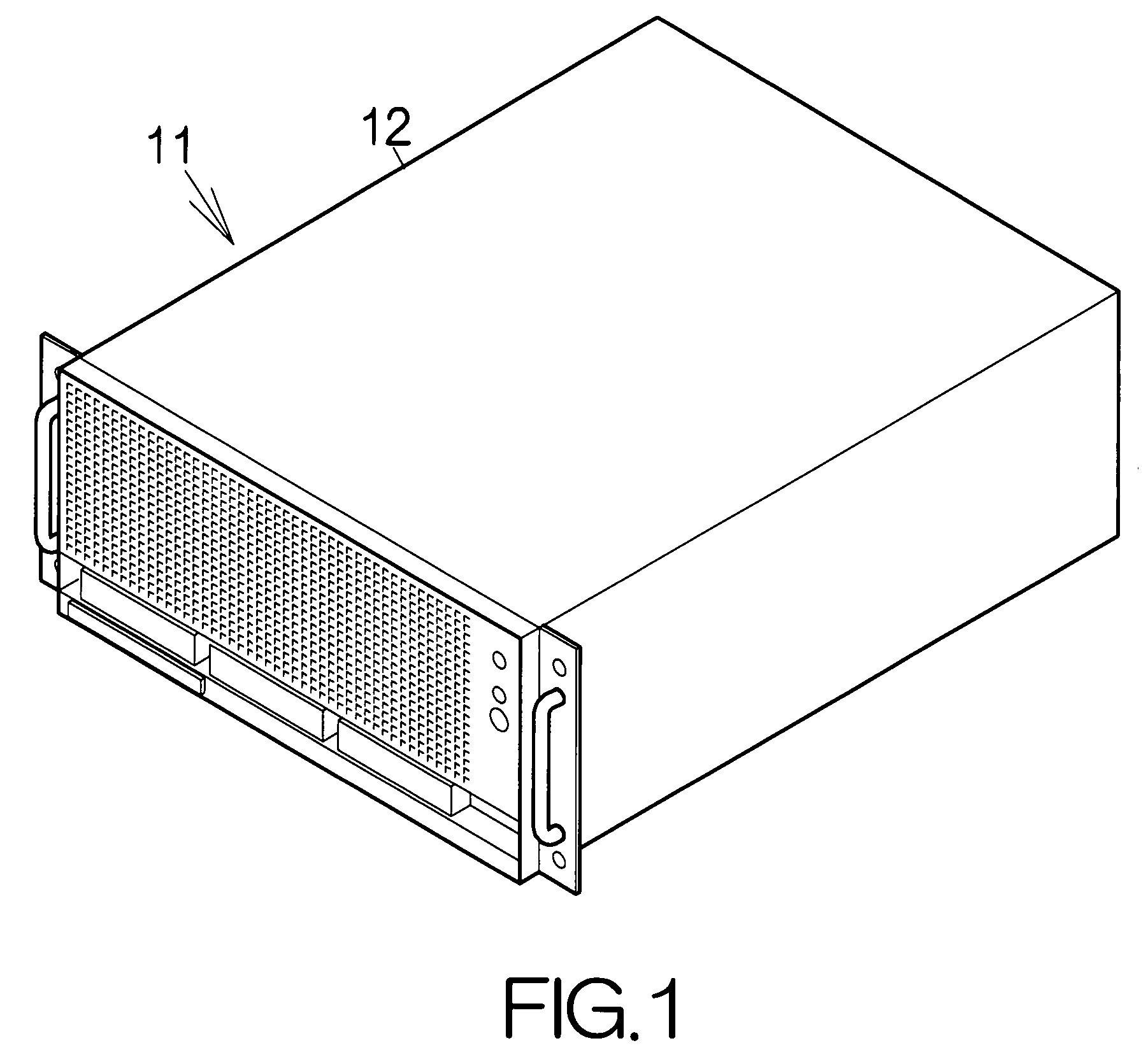
[0030]FIG. 1 schematically illustrates the structure of a server computer apparatus 11 as an electronic apparatus according to a specific example of the present invention. A server computer apparatus 11 includes an enclosure 12. The enclosure 12 defines an inner space. A motherboard is placed within the inner space, for example. The aftermentioned large-scale integrated (LSI) chip package, a memory and the like are mounted on the motherboard. The LSI chip package is designed to execute various kinds of processing based on a software program and / or data temporarily held in the memory, for example. The software program and / or data may be stored in a large-capacity storage such as a hard disk drive, HDD, likewise placed within the inner space. The server computer apparatus 11 is mounted on a rack, for example.
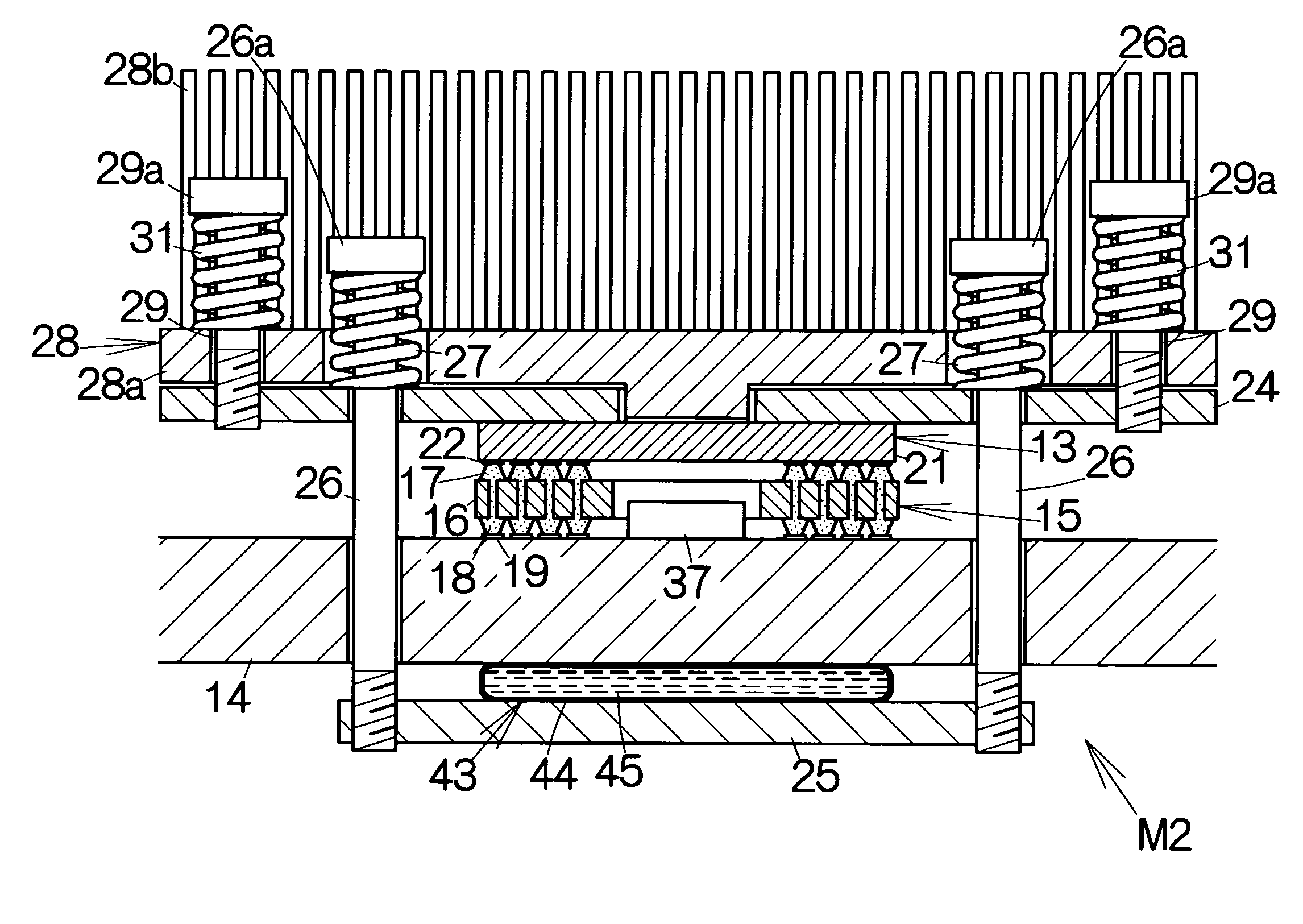
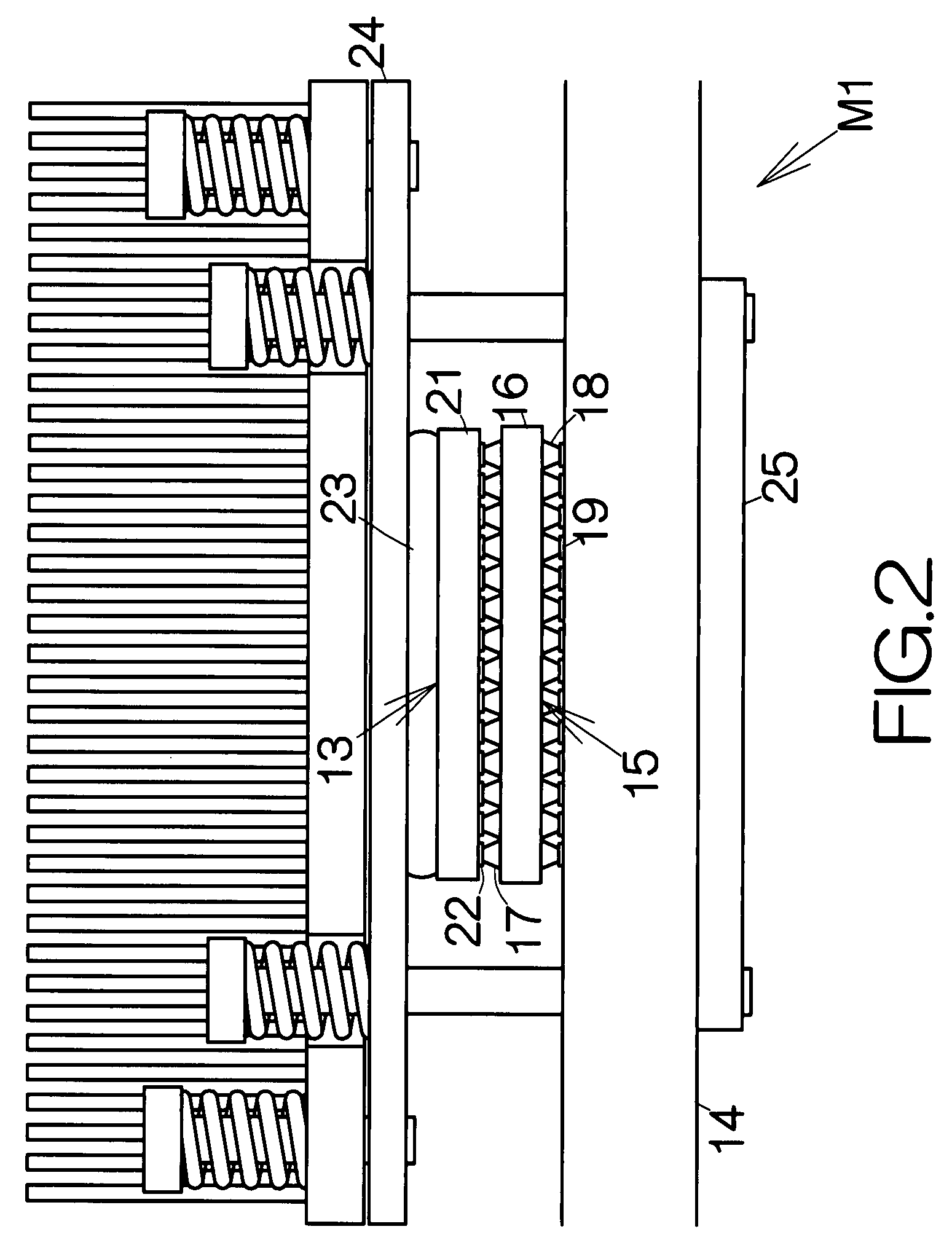
[0031]As shown in FIG. 2, a so-called land grid array (LGA) socket 15 is interposed between a LSI chip package 13 and a printed wiring board 14 in a motherboard M1 according to a ...
PUM
 Abstract
Description
Claims
Application Information