Printed circuit board unit and electronic apparatus

Inactive Publication Date: 2008-03-20
FUJITSU LTD
View PDF7 Cites 2 Cited by
  • Summary
  • Abstract
  • Description
  • Claims
  • Application Information

AI Technical Summary

Benefits of technology

[0006]It is accordingly an object of the present invention to provide a printed circuit board unit capable of reliably avoiding failure in electric conduction.
[0008]The printed circuit board unit allows transmission of an urging force from the static pressure member to the first board. The first board is subjected to the urging force toward the second board. The first electrically-conductive terminals are thus urged against the corresponding second electrically-conductive terminals. The static pressure member allows a uniform application of the urging force to the first board over a plane. Even if the urging plate is distorted, the urging force is uniformly applied to the first board. The equal urging force is applied to each of the first electrically-conductive terminals. All the first electrically-conductive terminals are thus reliably brought in contact with the corresponding second electrically-conductive terminals. This results in a reliable establishment of electric conduction between each of the first electrically-conductive terminals and the corresponding second electrically-conductive terminal. In the case where the urging force is unevenly applied, the first electrically-conductive terminal or terminals are allowed to receive a reduced urging force in a local area or areas. This often result in a failure in electric conduction between the first electrically-conductive terminal / terminals and the corresponding second electrically-conductive terminal / terminals.
[0013]Here, the printed circuit board unit may further comprise: an opening formed in the second board, the opening penetrating through the second board between the front surface and the back surface of the second board; third electrically-conductive terminals having flexibility arranged in a matrix on the back surface of the second board at a position around the opening, each of the third electrically-conductive terminals connected to the corresponding second electrically-conductive terminal; a third board having a front surface facing the back surface of the second board at a distance; fourth electrically-conductive terminals fixed on the front surface of the third board in a matrix, each of the fourth electrically-conductive terminals disengageably brought in contact with the corresponding third electrically-conductive terminal; and an electronic component mounted on the front surface of the third board, the electronic component disposed in the opening. The electronic component can be placed directly below the second board in this manner. The second board has a relatively large thickness to keep a sufficient strength regardless of the formation of the opening. The rigidity of the second board is also enhanced. The static pressure member serves to equalize the urging force. In the case where the opening is not formed in the second board, the second board may have a relatively small thickness. The second board can deform according to a distortion of the urging plate. Unevenness in the urging force can thus relatively be reduced.
[0015]Here, the printed circuit board unit may further comprise: an opening formed in the second board, the opening penetrating through the second board between the front surface and the back surface of the second board; and an electronic component mounted on the front surface of the first board, the electronic component disposed in the opening. The electronic component can be placed directly below the second board in this manner. The second board has a relatively large thickness to keep a sufficient strength regardless of the formation of the opening. The rigidity of the second board is also enhanced. The static pressure member serves to equalize the urging force.
[0017]The printed circuit board unit allows transmission of an urging force from the static pressure member to the first board in the same manner as described above during transmission of an urging force from the auxiliary static pressure member to the third board. The third board is subjected to the urging force toward the second board. The fourth electrically-conductive terminals are thus urged against the corresponding third electrically-conductive terminals. The auxiliary static pressure member allows a uniform application of the urging force to the third board over a plane. Even if the urging plate is distorted, the urging force is uniformly applied to the third board. The equal urging force is applied to each of the fourth electrically-conductive terminals. All the fourth electrically-conductive terminals are reliably brought in contact with the corresponding third electrically conductive terminals. This results in a reliable establishment of electronic conduction between each of the fourth electrically-conductive terminals and the corresponding third electrically-conductive terminal. The third board and the electronic component chip establish a so-called electronic component chip package. The second board can serve as a LGA socket interposed between a printed wiring board and the electronic component chip package, for example. The third board serves as a printed wiring board on which the electronic component chip package is mounted.
[0019]The printed circuit board unit allows transmission of an urging force from the static pressure member to the first board in the same manner as described above during transmission of an urging force from the auxiliary static pressure member to the third board. The third board is subjected to the urging force toward the second board. The fourth electrically-conductive terminals are thus urged against the corresponding third electrically-conductive terminals. The auxiliary static pressure member allows a uniform application of the urging force to the third board over a plane. Even if the urging plate is distorted, the urging force is uniformly applied to the third board. The equal urging force is applied to each of the fourth electrically-conductive terminals. All the fourth electrically-conductive terminals are reliably brought in contact with the corresponding third electrically conductive terminals. This results in a reliable establishment of electronic conduction between each of the fourth electrically-conductive terminals and the corresponding third electrically-conductive terminal. The third board and the electronic component chip establish a so-called electronic component chip package. The second board can serve as a LGA socket interposed between a printed wiring board and the electronic component chip package, for example. The third board serves as a printed wiring board on which the electronic component chip package is mounted. Moreover, the electronic component can be placed directly below the second board. The second board has a relatively large thickness to keep a sufficient strength regardless of the formation of the opening. The rigidity of the second board is also enhanced. The static pressure member serves to equalize the urging force.

Problems solved by technology

This often result in a failure in electric conduction between the first electrically-conductive terminal / terminals and the corresponding second electrically-conductive terminal / terminals.

Method used


Image

  • Printed circuit board unit and electronic apparatus
  • Printed circuit board unit and electronic apparatus
  • Printed circuit board unit and electronic apparatus

Examples


Embodiment Construction

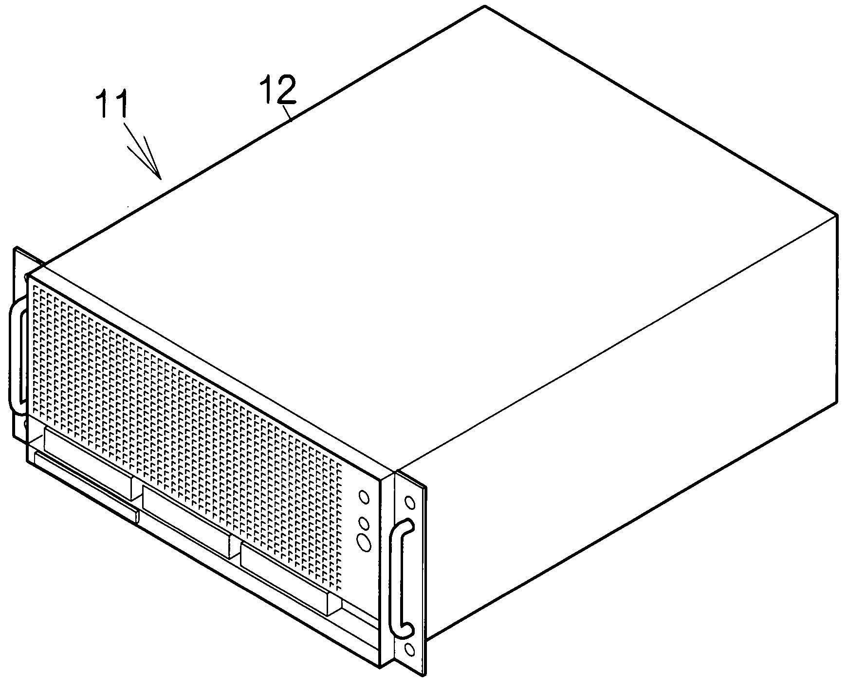
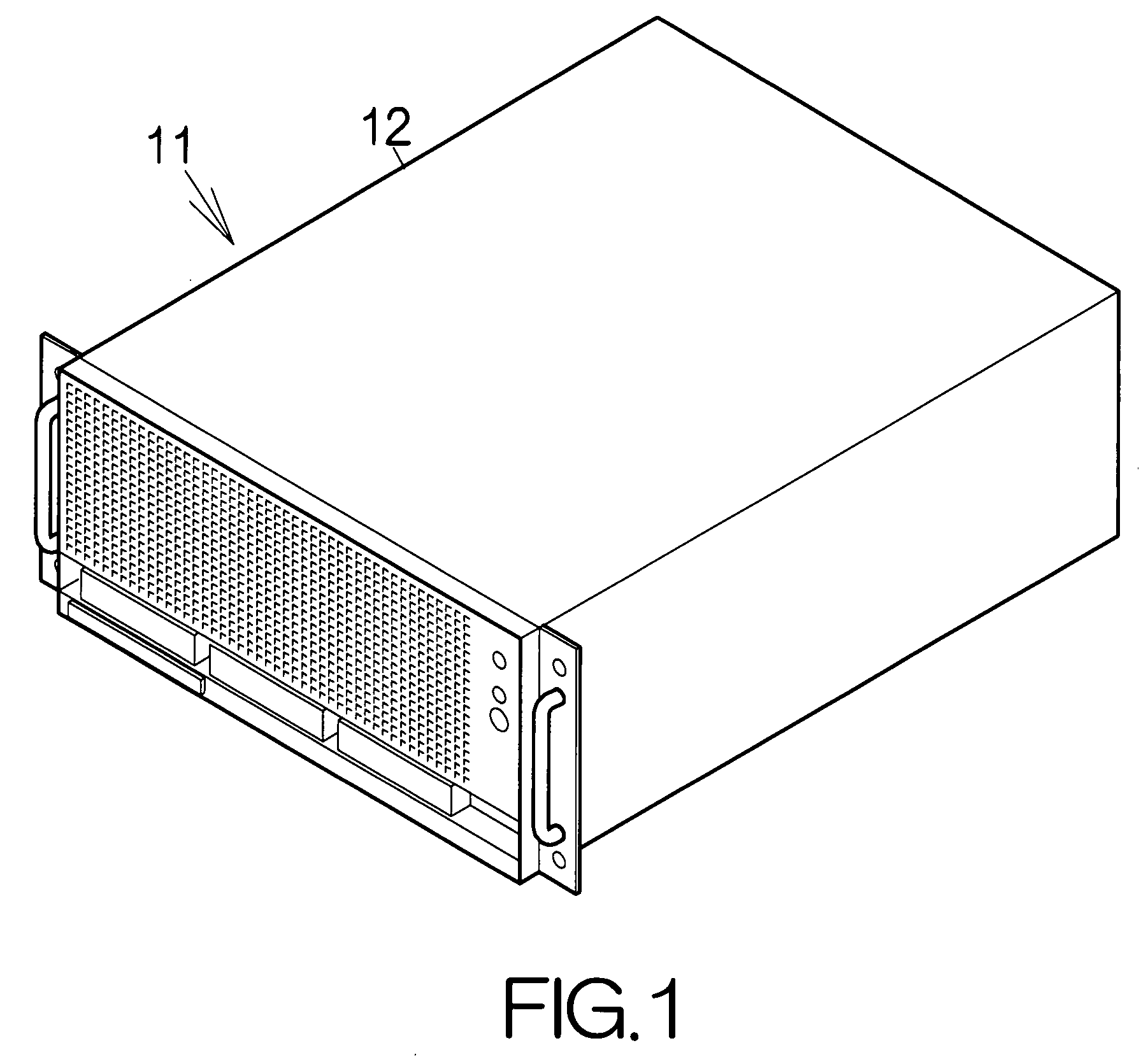
[0030]FIG. 1 schematically illustrates the structure of a server computer apparatus 11 as an electronic apparatus according to a specific example of the present invention. A server computer apparatus 11 includes an enclosure 12. The enclosure 12 defines an inner space. A motherboard is placed within the inner space, for example. The aftermentioned large-scale integrated (LSI) chip package, a memory and the like are mounted on the motherboard. The LSI chip package is designed to execute various kinds of processing based on a software program and / or data temporarily held in the memory, for example. The software program and / or data may be stored in a large-capacity storage such as a hard disk drive, HDD, likewise placed within the inner space. The server computer apparatus 11 is mounted on a rack, for example.

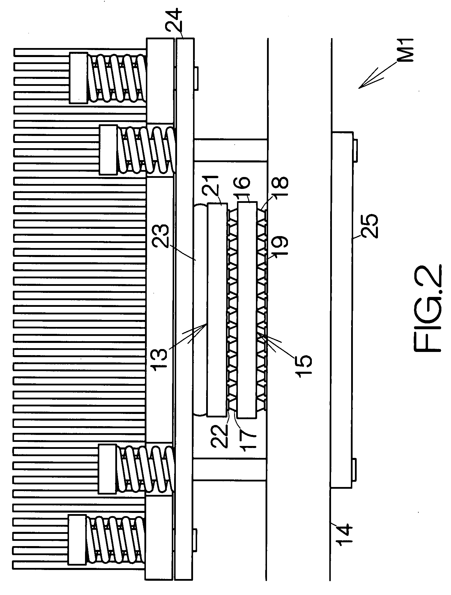
[0031]As shown in FIG. 2, a so-called land grid array (LGA) socket 15 is interposed between a LSI chip package 13 and a printed wiring board 14 in a motherboard M1 according to a ...


PUM


Abstract

A printed circuit board unit includes a first board and a second board. First electrically-conductive terminals are fixed and exposed on the front surface of the first board within a specific area of the first board in a matrix. Second electrically-conductive terminals are arranged in a matrix and supported on the front surface of the second board. The second electrically-conductive terminals have flexibility. Each of the second electrically-conductive terminals is disengageably brought in contact with the corresponding first electrically-conductive terminal. A static pressure member is received on the back surface of the first board within an area corresponding to the specific area to generate a static pressure. An urging plate is overlaid on the static pressure member so that the static pressure member is interposed between the urging plate and the first board. The urging plate exhibits an urging force applied to the first board toward the second board.

Description

BACKGROUND OF THE INVENTION[0001]1. Field of the Invention[0002]The present invention relates to a printed circuit board unit including first electrically-conductive terminals fixed and exposed on a board in a matrix and second electrically-conductive terminals having flexibility arranged in a matrix, for example. The second electrically-conductive terminals are disengageably brought in contact with the corresponding first electrically-conductive terminals.[0003]2. Description of the Prior Art[0004]A land grid array (LGA) socket is well known as disclosed in “Land grid array sockets for server applications”, J. S. Corbin et al., IBM J. RES. & DEV., Vol. 46, No. 6, p. 763-778, November, 2002, for example. The LGA socket is utilized to mount a large scale integrated (LSI) package. The LGA socket has lower electrically-conductive terminals arranged on the lower surface of a socket board to be respectively received on electrically-conductive pads on a printed wiring board. Upper electri...

Claims


Application Information

Patent Timeline
IPC IPC(8): H05K7/12H01L23/32H01R4/48H05K1/14
CPCH01L23/433H01L23/4338H01R13/2414H05K1/0231H05K3/0058H05K3/325H05K2201/0314H01L2924/0002H05K2201/10515H05K2201/10719H05K2201/2009H01L2924/00
Inventor MORITA, YOSHIHIRO
Owner FUJITSU LTD
Why Eureka
Try Eureka