Supercharge Your Innovation With Domain-Expert AI Agents!

IC package having IC-to-PCB interconnects on the top and bottom of the package substrate

a technology of ic-to-pcb interconnection and package substrate, which is applied in the field of ic packages, can solve the problems of increasing the cost of further miniaturizing the area of bond pads and spacing, and the unwieldy nature of conventional package substrates, and achieves the effect of high input/outpu

Active Publication Date: 2010-08-10
NVIDIA CORP
View PDF4 Cites 12 Cited by
  • Summary
  • Abstract
  • Description
  • Claims
  • Application Information

AI Technical Summary

Benefits of technology

The present technology is about creating integrated circuit (IC) packages with a high input / output (I / O) density. The IC package includes a package substrate, an interface stratum, and an IC die. The IC die has a microelectronic circuit with a plurality of inputs and outputs, which are electrically coupled to the package substrate and the interface stratum. The package substrate has connection regions that allow for the electrical coupling of the IC die and the interface stratum. The technology also includes a printed circuit board assembly (PCBA) with an IC die, a PCB, and one or more interface strums. The package substrate has connection pads that are coupled to the IC die and the PCB, and the interface stratum has connection pads that are coupled to the PCB. The method of fabricating the IC package involves electrically and mechanically coupling the pads on the IC die to the pads on the package substrate, and then electrically coupling the pads on the interface stratum to the pads on the package substrate.

Problems solved by technology

For reliable connection with a PCB, it becomes increasingly more expensive to further miniaturize the area of the bond pads and spacing between the pads.
Accordingly, at some point conventional package substrates become unwieldy large due to the large number of connection regions that must be fabricated on the surface that is coupled to the PCB.

Method used


Image

  • IC package having IC-to-PCB interconnects on the top and bottom of the package substrate
  • IC package having IC-to-PCB interconnects on the top and bottom of the package substrate
  • IC package having IC-to-PCB interconnects on the top and bottom of the package substrate

Examples


Embodiment Construction

[0016]Reference will now be made in detail to the embodiments of the invention, examples of which are illustrated in the accompanying drawings. While the invention will be described in conjunction with these embodiments, it will be understood that they are not intended to limit the invention to these embodiments. On the contrary, the invention is intended to cover alternatives, modifications and equivalents, which may be included within the scope of the invention as defined by the appended claims. Furthermore, in the following detailed description of the present invention, numerous specific details are set forth in order to provide a thorough understanding of the present invention. However, it is understood that the present invention may be practiced without these specific details. In other instances, well-known methods, procedures, components, and circuits have not been described in detail as not to unnecessarily obscure aspects of the present invention.

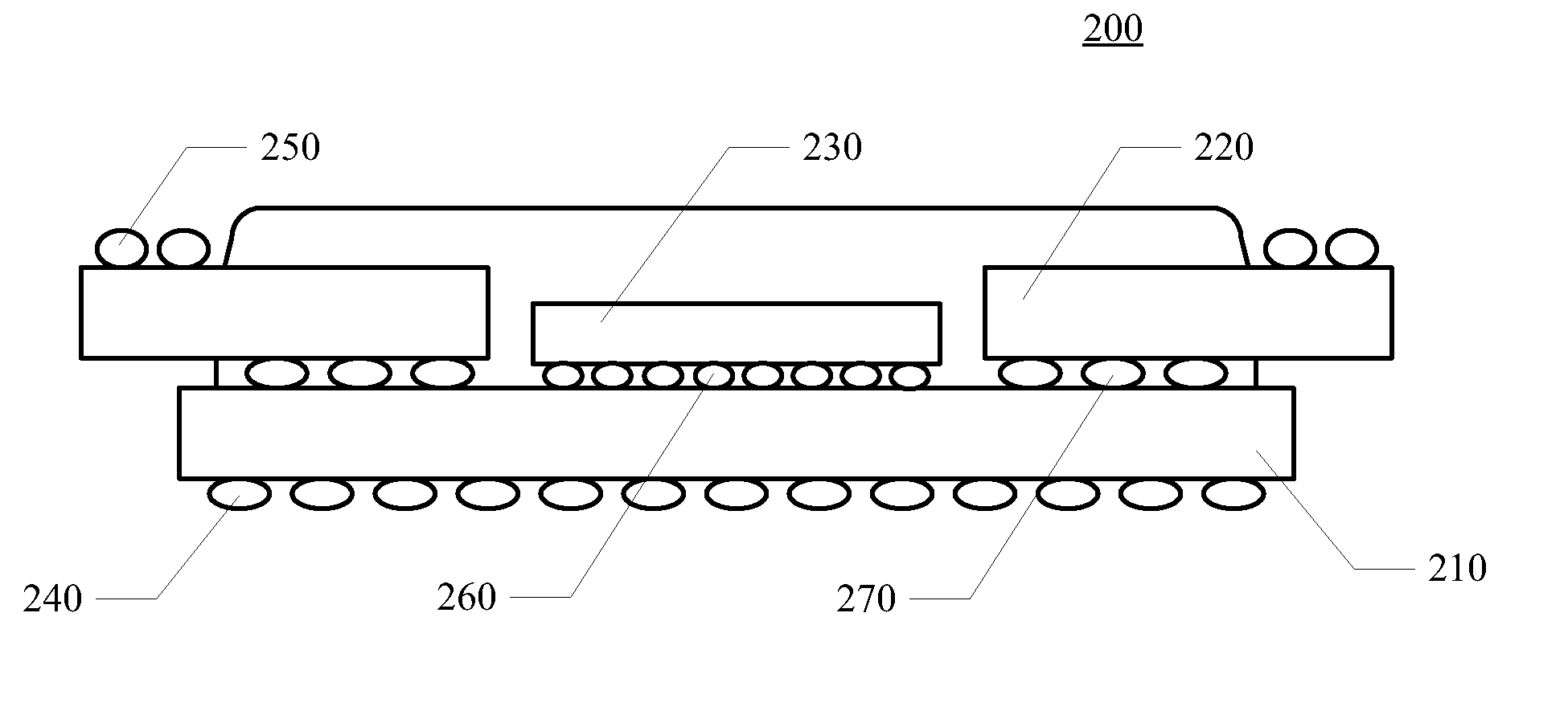
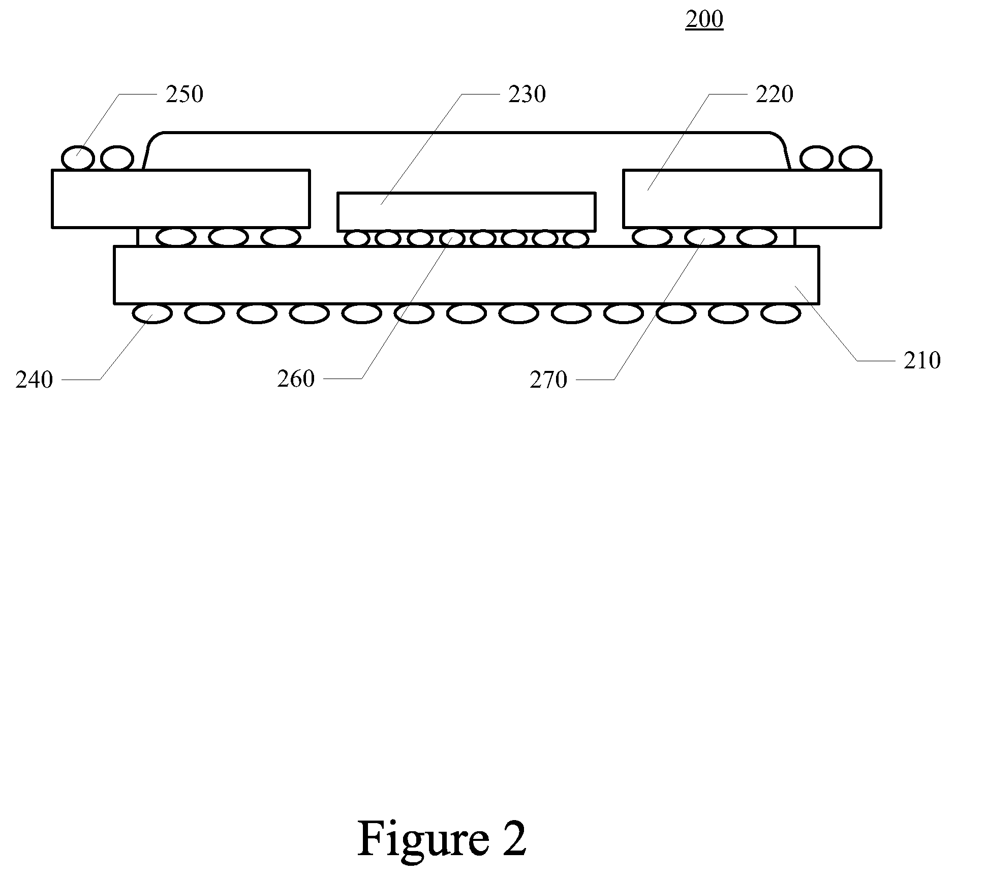
[0017]Referring to FIG. 2, a...


PUM


Abstract

An integrated circuit package, according to one embodiment, includes a package substrate, an interface stratum and an integrated circuit die. Both the IC die and interface stratum are disposed on the package substrate. The integrated circuit die includes a microelectronic circuit having a plurality of inputs and outputs. A first set of the inputs and outputs are electrically coupled to a plurality of package-to-circuit connection regions on the package substrate. A second set of input and outputs are electrically coupled through the package substrate to package-to-circuit connection regions on the interface stratum.

Description

BACKGROUND OF THE INVENTION[0001]As microelectronic circuit designs become ever larger, larger integrated circuit packages are also necessary as a result of the extra signal and supply interconnections of the larger microelectronic circuits. Referring to FIG. 1, a printed circuit board assembly, according to the conventional art, is shown. The PCBA 100 typically includes a printed circuit board 110 and a plurality of integrated circuit (IC) packages and one or more discrete electronic components. Conventional IC packages include an integrated circuit (IC) die 120 and a package substrate 130. The IC package may also include an encapsulant 140, thermal dissipation element or combination thereof to provide thermal dissipation, electrical, mechanical, and / or environmental protection. The package substrate 130 is adapted to electrically couple the IC die 120 to a printed circuit board (PCB) 110. In particular, the IC die 120 includes a plurality of connection pads disposed on a first sur...

Claims


Application Information

Patent Timeline
Patent Type & Authority Patents(United States)
IPC IPC(8): H01L23/48
CPCH01L24/73H01L23/49833H01L23/49816H01L2224/16225H01L24/16H01L2224/16H01L2224/48464H01L2924/01082H01L2924/14H01L2924/1433H01L2924/15162H01L2924/15311H01L2924/15331H01L2924/19107H01L24/48H01L2924/01033H01L2924/181H01L2924/00014H01L2924/00012H01L2224/45099H01L2224/45015H01L2924/207
Inventor HUNTER, MATTHEW A
Owner NVIDIA CORP
Features
  • R&D
  • Intellectual Property
  • Life Sciences
  • Materials
  • Tech Scout
  • Unparalleled Data Quality
  • Higher Quality Content
  • 60% Fewer Hallucinations
Learn More