Defective conductive surface pad repair for microelectronic circuit cards

Inactive Publication Date: 2012-09-13
I3 ELECTRONICS
View PDF1 Cites 25 Cited by
  • Summary
  • Abstract
  • Description
  • Claims
  • Application Information

AI Technical Summary

Benefits of technology

[0025]It is, therefore, also a primary object of the invention to enhance the art of circuitized substrate manufacture in whic

Problems solved by technology

The previously disclosed United States patents and published patent applications fail to apply conductive paste to repair and rebuild damaged and defect

Method used


Image

  • Defective conductive surface pad repair for microelectronic circuit cards
  • Defective conductive surface pad repair for microelectronic circuit cards
  • Defective conductive surface pad repair for microelectronic circuit cards

Examples


Embodiment Construction

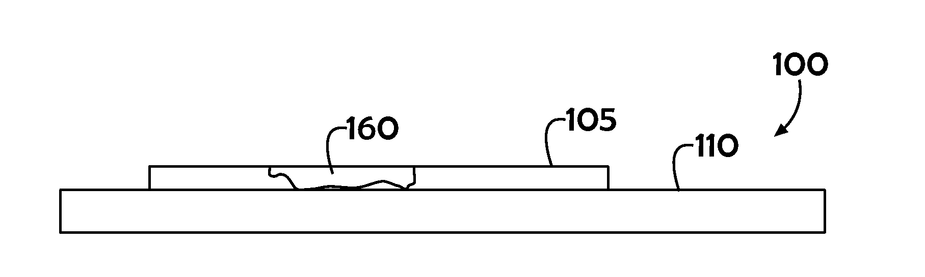
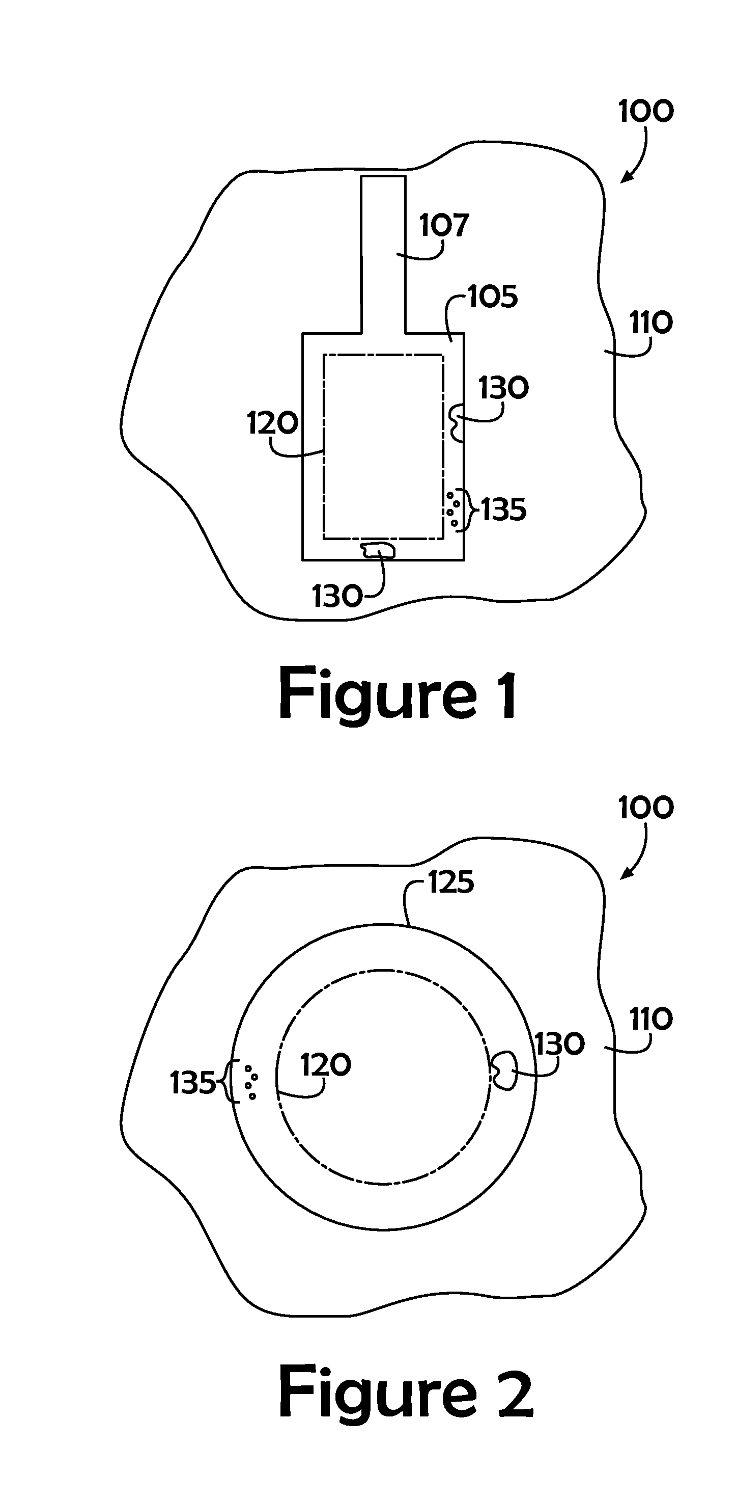
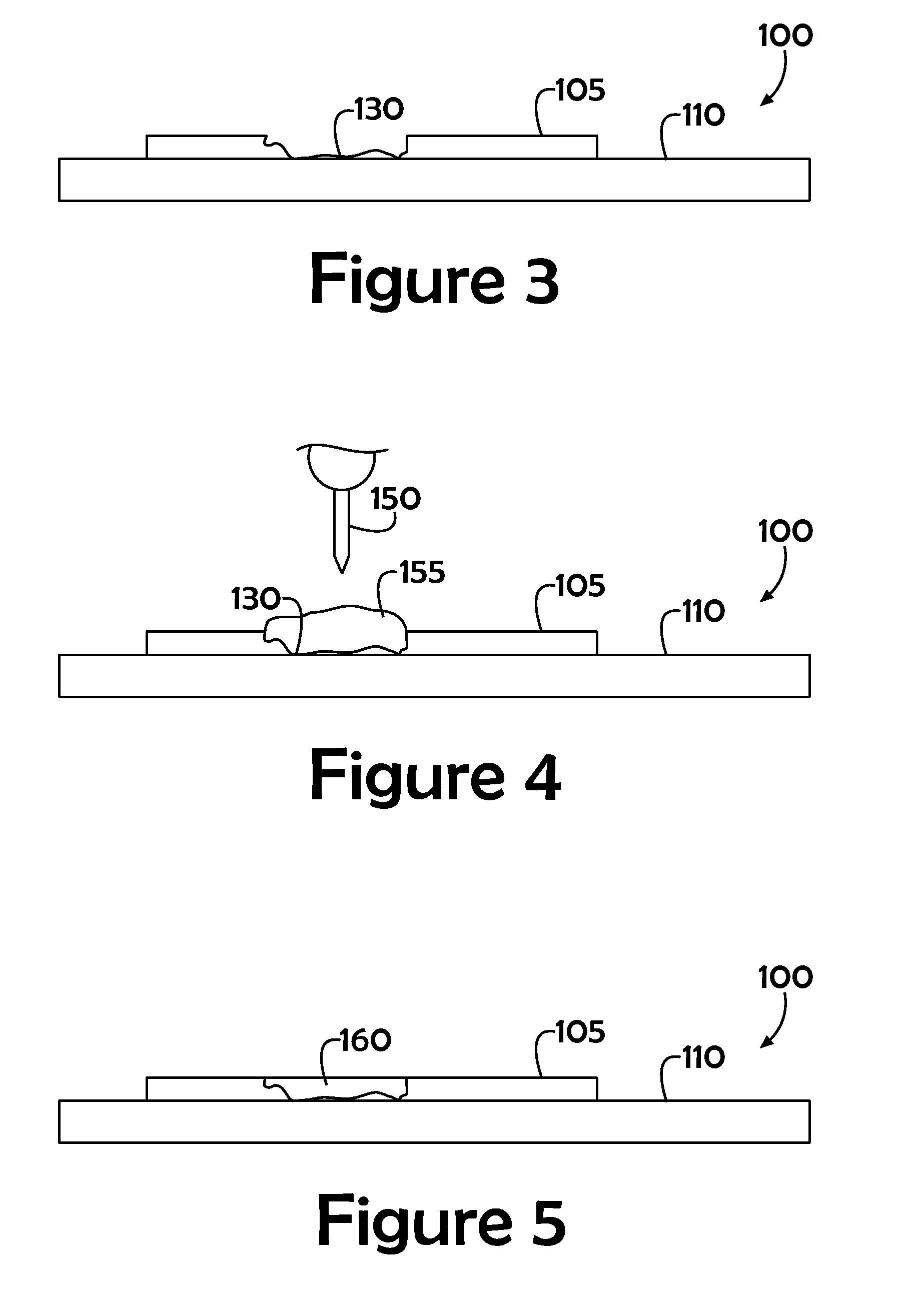
[0033]Generally speaking, the present invention is a method and structure for repairing or rebuilding defective interconnect pads of substrate surfaces utilizing an electrically conductive adhesive (ECA). The connection repair or rebuild is achieved by disposing a quantity of ECA on the defective metallized surfaces. The use of an ECA on the defective connecting points enables the pad to pass physical and electrical inspection routines as an alternative to being scrapped.

[0034]For a better understanding of the present invention, together with other and further objects, advantages and capabilities thereof, reference is made to the following disclosure and appended claims.

[0035]By the term “circuitized substrate” as used herein is meant to define a structure including at least one dielectric layer having at least one surface having thereon at least one circuit. Examples of dielectric materials suitable for use in such structures include fiberglass-reinforced or non-reinforced epoxy re...


PUM

PropertyMeasurementUnit
Temperatureaaaaaaaaaa
Particle sizeaaaaaaaaaa

Abstract

An electrically conductive adhesive (ECA) for repairing electrically conductive pad and trace interconnects and a method of repairing interconnect locations. The method of repairing at least one defect within the area of electrically conductive circuitized substrate traces and pads outside of a pristine center area incorporates an ECA and a forming gas plasma. The ECA contains a mixture of components that allow the adhesive to be adapted to specific requirements. Curing the adhesive results in effective electrical connections being formed between the adhesive and the base pad so that the metallurgies of the conductors and of the ECA are effectively combined to engage and repair the conductor defect.

Description

FIELD OF INVENTION[0001]The present invention relates to defect repair using electrically conductive adhesive (ECA) and, more specifically, to an ECA that can be used to repair multiple, disparate interconnect locations, such as Z-interconnect surface pads, circuit board land areas, printed wiring board pads, circuitized substrate pads and the like.BACKGROUND OF THE INVENTION[0002]Printed circuit boards (PCBs), chip carriers, and similar circuitized substrate products typically present one and often two opposing planar surfaces on which electronic components such as semiconductor chips, resistors, capacitors, modules, etc. are to be mounted. As known, PCBs may also have one or more chip carriers (each including one or more chips as part thereof) mounted thereon, while such chip carriers in turn may have the chips mounted to the substrates thereof, typically utilizing wire-bond or solder reflow technologies.[0003]Circuit paths for these components are also typically provided by formi...

Claims


Application Information

Patent Timeline
IPC IPC(8): H05K1/00H01B1/00H01B1/04H05K1/11B23K31/02H01B1/02B82Y30/00
CPCH05K1/095H05K3/225B23K2201/42H05K2203/095B23K1/0016H05K2203/0126B23K2101/42
Inventor MATIENZO, LUIS J.PITELY, SUSANCARD, NORMAN A.
Owner I3 ELECTRONICS
Why Eureka
Try Eureka