Programmable impedance matching circuit and method

a technology of impedance matching and circuit, applied in waveguide devices, antennas, electrically long antennas, etc., can solve problems such as interference, impedance mismatch, jitter noise, etc., to improve signal integrity and improve signal integrity

Inactive Publication Date: 2006-12-05
IBM CORP
View PDF23 Cites 25 Cited by
  • Summary
  • Abstract
  • Description
  • Claims
  • Application Information

AI Technical Summary

Benefits of technology

[0011]According to an aspect of the invention, a microelectronic circuit is provided for improving signal integrity at a transmission line. The circuit includes a programmably adjustable impedance matching circuit coupled to a transmiss

Problems solved by technology

One challenge is the presence of reflection along transmission lines that carry data between components of the system.
Many things can lead to impedance mismatch and, therefore, reflection along a transmission line.
Wiring and interconnections in the microelectronic package and even printed wiring boards and passive components are all subject to variations in the manufacturing process and changes due to temperature, thus contributing to impedance mismatch and jitter noise.
Depending on the strength of the transmitted signal and the ratio of the transmitted signal to the reflected signal, the transmitted signal and the reflected signal may either cancel each other out or otherwise interfere.
Although these concerns are addressed somewhat by use of on-board termination resistors to terminate transmission lines, there are problems that hinder achievement of this goal.
Difficulties in chip design arise when the length of on-chip wiring between input output (I/O) devices and the bonding pads causes such on-chip wiring to act more like a transmission line, affecting signal integrity.
The impedance of the on-chip wiring, as well as its length in such instances becomes considerable due to layout and pad limitation.
The problem is further aggravate

Method used


Image

  • Programmable impedance matching circuit and method
  • Programmable impedance matching circuit and method
  • Programmable impedance matching circuit and method

Examples


Embodiment Construction

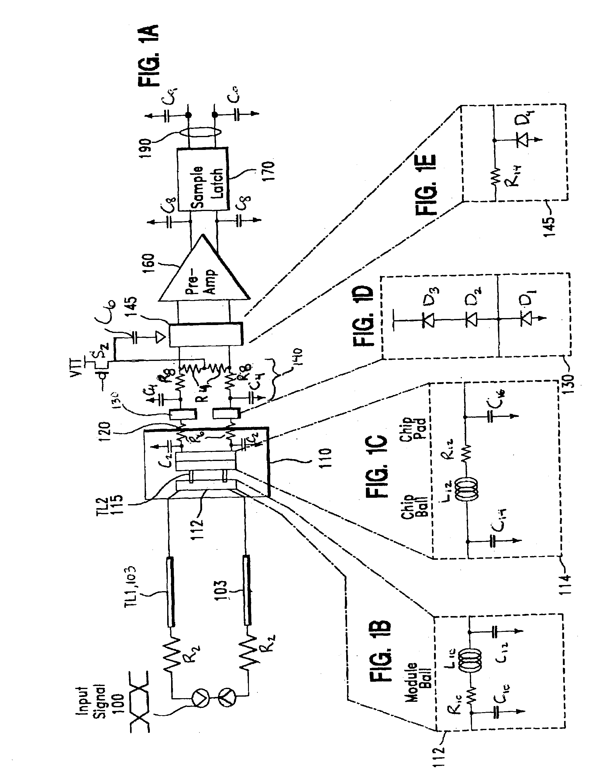
[0031]In systems including many active electronic components, signals are transmitted from a transmitter formed on one chip or component to a receiver formed on another chip or component through transmission lines that connect the two chips or components. FIGS. 1A and 2A respectively illustrate such receiver and transmitter, modeled as networks. It is important to study the structure of such networks, in order to understand the source of signal reflections, since the invention provides ways of reducing impedance mismatches and reflections.

[0032]In the receiver network of FIG. 1A, a differential signal 100 having true and complementary signals is coupled through a pair of source resistors R2 to a pair of transmission lines (TL1) 103, each having a characteristic impedance Z0. Each transmission line (TL1) 103, in turn, is coupled to the receiver through a package 110, e.g. a ball grid array package, which includes a module ball 112, for which a circuit equivalent is shown in FIG. 1B m...


PUM


Abstract

As disclosed herein, a microelectronic circuit and method are provided for improving signal integrity at a transmission line. The circuit includes a programmably adjustable impedance matching circuit which is coupled to a transmission line which includes a programmably adjustable inductive element. The programmably adjustable impedance matching circuit is desirably provided on the same chip as a receiver or transmitter to which the transmission line is coupled, or alternatively, on an element packaged together with the chip that includes the receiver or transmitter. The impedance of the programmably adjustable impedance matching circuit is adjustable in response to control input to improve signal integrity at the transmission line.

Description

BACKGROUND OF INVENTION[0001]The present invention relates to fabrication of microelectronic circuits and more particularly to a structure and method for programmably adjusting a matched impedance to reduce signal reflection at an interface to a transmission line.[0002]The continuous increase in the speed and complexity of digital communication systems leads to a strong demand for improved methods of data transmission in these systems. One challenge is the presence of reflection along transmission lines that carry data between components of the system. A reflection is a return of energy (i.e. electromagnetic energy) caused by an impedance mismatch occurring along a transmission line. Stated another way, any pulse or signal propagating along a transmission line will reflect at any point where the transmission line becomes different.[0003]Many things can lead to impedance mismatch and, therefore, reflection along a transmission line. For example, variations in manufacturing process ca...

Claims


Application Information

Patent Timeline
IPC IPC(8): H03H7/38
CPCH03H7/38
Inventor HSU, LOUIS L.NATONIO, JOSEPHSTORASKA, DANIEL W.WASHBURN, WILLIAM F.
Owner IBM CORP
Why Eureka
Try Eureka