Method of manufacturing vertical light emitting device

a technology manufacturing method, which is applied in the direction of semiconductor devices, basic electric elements, electrical apparatus, etc., can solve the problems of light emitting device cracks in the emissive layer that cannot normally be used, current may leak through the sidewalls of the conventional vertical light emitting device, and the manufacturing method is certain. to achieve the effect of reducing or preventing cracks and reducing current leakag

Active Publication Date: 2010-08-24
SAMSUNG ELECTRONICS CO LTD
View PDF4 Cites 13 Cited by
  • Summary
  • Abstract
  • Description
  • Claims
  • Application Information

AI Technical Summary

Benefits of technology

[0023]Example embodiments provide a method of manufacturing a vertical light emitting device which may reduce or prevent a crack from occurring when a laser lift off (LLO) method is performed and in which a passivation layer for reducing or preventing current leakage may be formed more easily and reliably.

Problems solved by technology

However, in a conventional vertical light emitting device having the above structure, current may leak through the sidewalls of the conventional vertical light emitting device.
The conventional manufacturing method has certain recognized problems.
A light emitting device having cracks in the emissive layer cannot normally be used.
Accordingly, the characteristics of the light emitting device may deteriorate.

Method used


Image

  • Method of manufacturing vertical light emitting device
  • Method of manufacturing vertical light emitting device
  • Method of manufacturing vertical light emitting device

Examples


Embodiment Construction

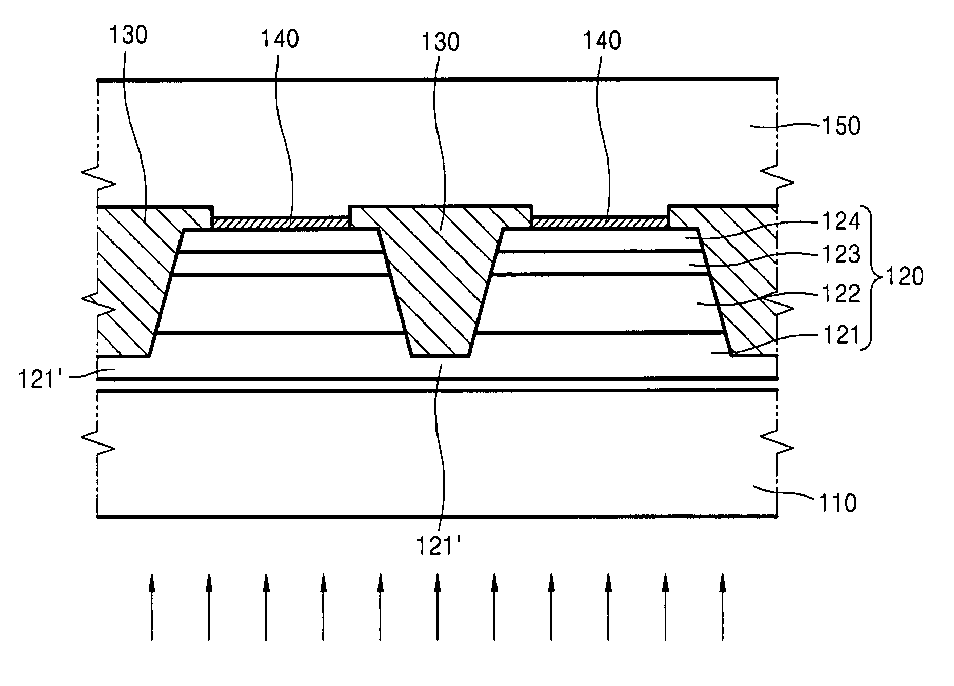
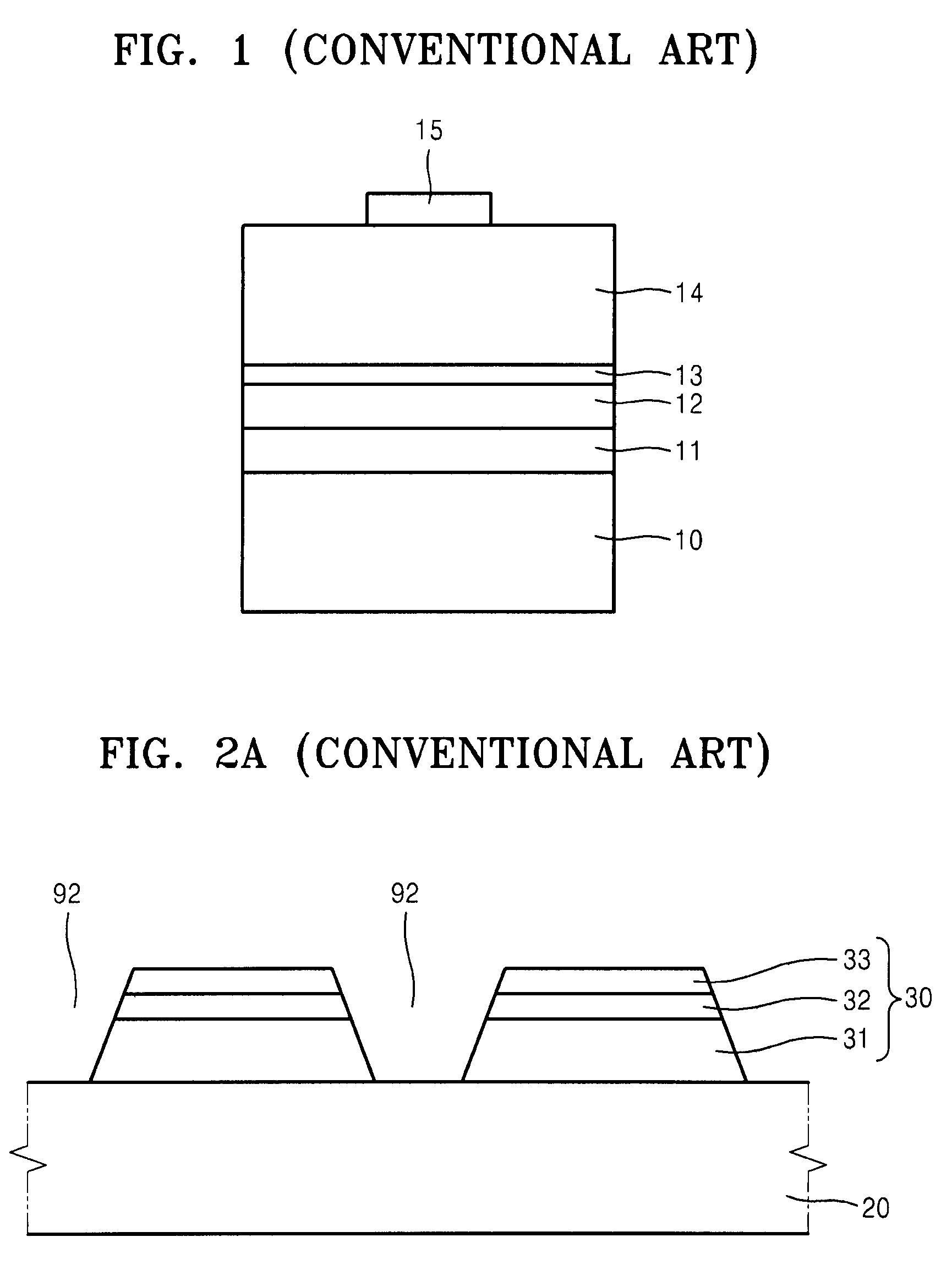
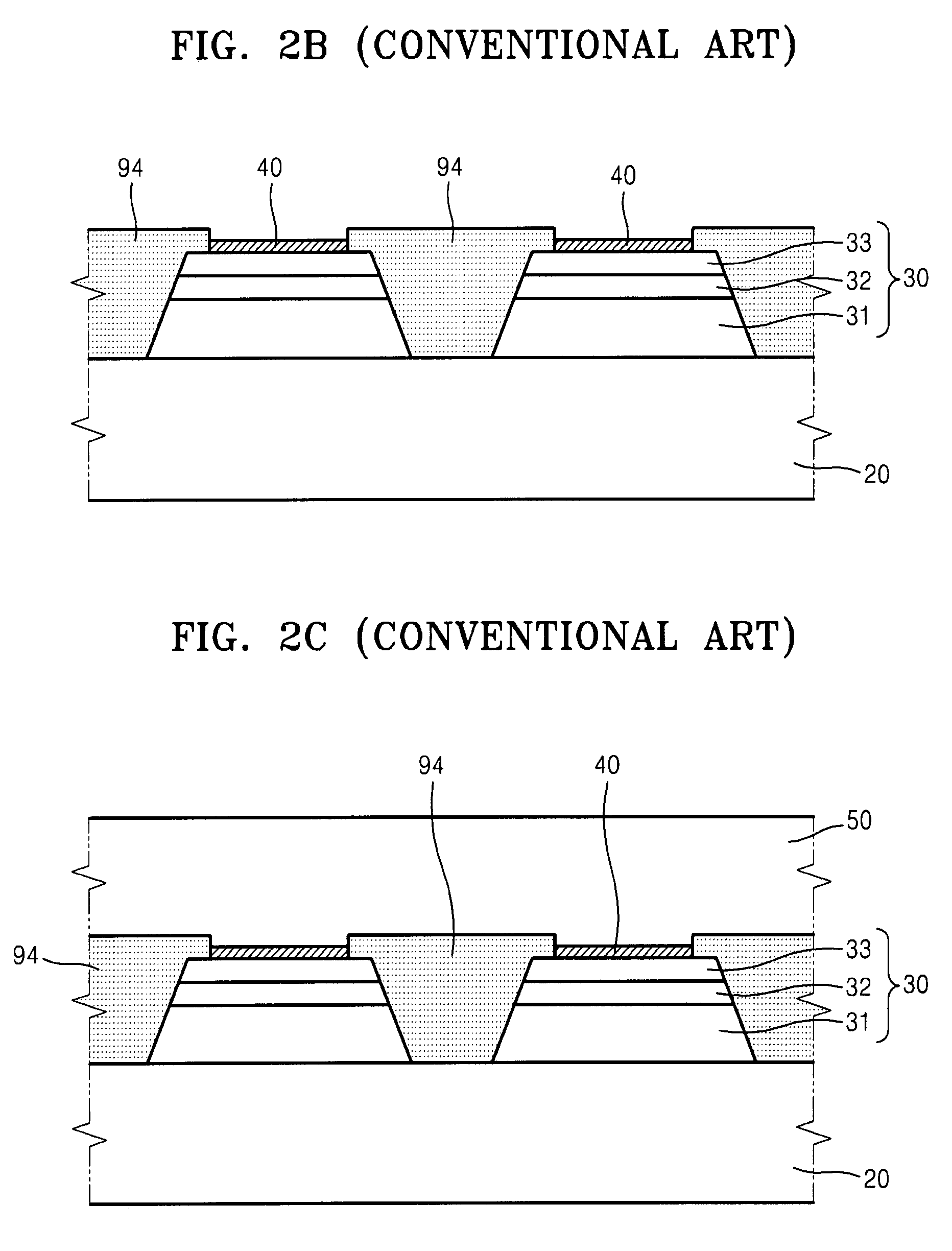
[0045]Reference will now be made in detail to example embodiments, examples of which are illustrated in the accompanying drawings. However, example embodiments are not limited to the embodiments illustrated hereinafter, and the embodiments herein are rather introduced to provide easy and complete understanding of the scope and spirit of example embodiments. In the drawings, the thicknesses of layers and regions are exaggerated for clarity.

[0046]It will be understood that when an element or layer is referred to as being “on,”“connected to” or “coupled to” another element or layer, it may be directly on, connected or coupled to the other element or layer or intervening elements or layers may be present. In contrast, when an element is referred to as being “directly on,”“directly connected to” or “directly coupled to” another element or layer, there are no intervening elements or layers present. Like reference numerals refer to like elements throughout. As used herein, the term “and / or...


PUM


Abstract

Provided is a method of manufacturing a vertical light emitting device. The method of manufacturing the vertical light emitting device may include forming an emissive layer including a n-type semiconductor layer, an active layer, and a p-type semiconductor layer on a substrate, forming a first trench dividing the emissive layer into light emitting device units in which the emissive layer remains on the lower part of the first trench to a desired, or alternatively, a predetermined thickness, forming a passivation layer on the emissive layer, forming a p-type electrode on the p-type semiconductor layer of the emissive layer, forming a metal supporting layer on the passivation layer and the p-type electrode, removing the substrate, removing a remaining portion of the emissive layer when the surface of the emissive layer is exposed by removing the substrate, forming a n-type electrode on the n-type semiconductor layer of the emissive layer, and cutting the metal supporting layer to divide the emissive layer into the light emitting device units.

Description

PRIORITY STATEMENT[0001]This application claims priority under 35 USC §119 to Korean Patent Application No. 2006-0112449, filed on Nov. 14, 2006, in the Korean Intellectual Property Office (KIPO), the entire contents of which are herein incorporated by reference.BACKGROUND[0002]1. Field[0003]Example embodiments relate to a method of manufacturing a vertical light emitting device including a passivation layer formed on a sidewall of the vertical light emitting device which may prevent current leakage.[0004]2. Description of Related Art[0005]Light emitting devices (e.g., light emitting diodes (LEDs)) are widely used for transmitting, recording, and / or reading data in communication devices (e.g., optical communication devices), for example, compact disc players (CDPs), digital versatile disc players (DVDPs), or similar. Light emitting devices are also widely applied to components for large-sized electronic sign boards and liquid crystal display devices, for example, backlights. Current...

Claims


Application Information

Patent Timeline
Patent Type & Authority Patents(United States)
IPC IPC(8): H01L21/00H01L33/00H01L33/44
CPCH01L33/0079H01L33/44H01L33/0093
Inventor KIM, HYUN-SOOKIM, KYOUNG-KOOKKIM, HYUNG-KUNCHOI, KWANG-KILEE, JEONG-WOOK
Owner SAMSUNG ELECTRONICS CO LTD
Why Eureka
Try Eureka