Electronic component and method for manufacturing same
a technology of electronic components and manufacturing methods, applied in the field of electronic components, can solve the problems of easy cracking during firing, and achieve the effect of reducing or preventing cracking and low esr
- Summary
- Abstract
- Description
- Claims
- Application Information
AI Technical Summary
Benefits of technology
Problems solved by technology
Method used
Image
Examples
first preferred embodiment
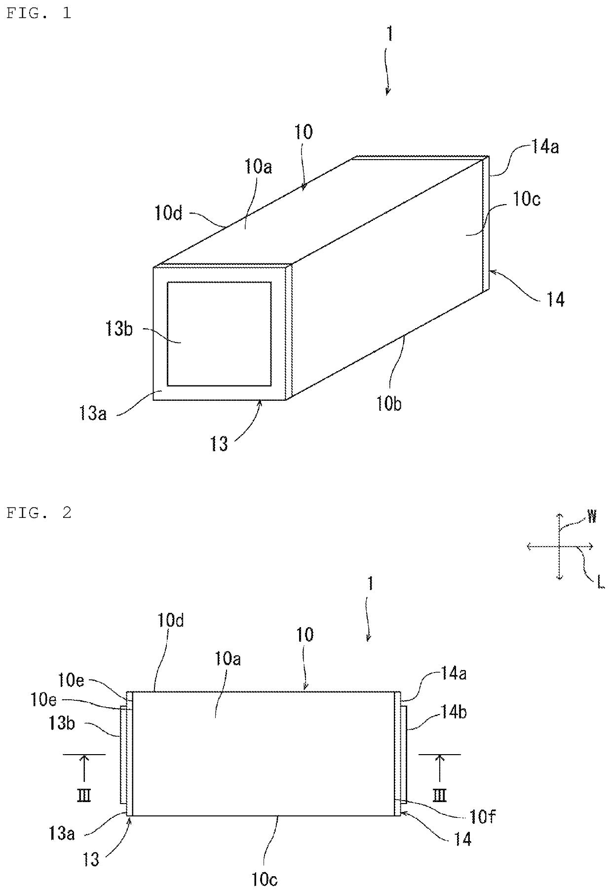
[0043]FIG. 1 is a schematic perspective view of an electronic component of a first preferred embodiment of the present invention. FIG. 2 is a schematic plan view of the electronic component of the first preferred embodiment. FIG. 3 is a schematic cross-sectional view taken on line III-III of FIG. 2.
[0044]An electronic component 1 preferably includes a rectangular parallelepiped electronic component main body 10. The electronic component main body 10 includes a first principal surface 10a and a second principal surface 10b (refer to FIG. 3), a first side surface 10c and a second side surface 10d (refer to FIG. 2), and a first end surface 10e and a second end surface 10f. The first principal surface 10a and the second principal surface 10b each extend along a length direction L and a width direction W. The first side surface 10c and the second side surface 10d each extend along a laminating direction T and the length direction L. The first end surface 10e and the second end surface 10...
second preferred embodiment
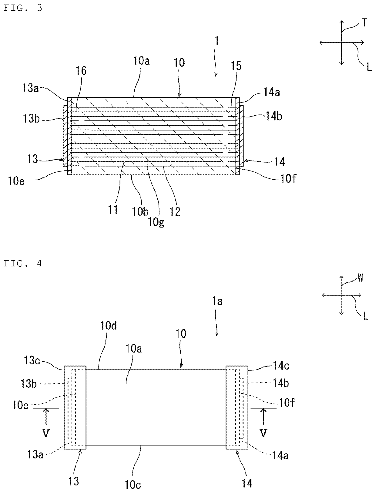
[0114]FIG. 4 is a schematic plan view of the electronic component of a second preferred embodiment of the present invention. FIG. 5 is a schematic cross-sectional view taken on line V-V of FIG. 4.
[0115]The electronic component 1a shown in FIG. 4 and FIG. 5 is preferably different from the electronic component 1 according to the first preferred embodiment in that the first external electrode 13 further includes a fifth conductive layer 13c covering the conductive layers 13a and 13b, and the second external electrode 14 further includes a sixth conductive layer 14c covering the second conductive layer and the fourth conductive layer 14a and 14b. The fifth conductive layer 13c is formed to range from above the first end surfaces 10e on which the first conductive layer and the third conductive layers 13a, 13b are formed on the first principal surface 10a and the second principal surface 10b and the first side surface 10c and the second side surface 10d. The sixth conductive layer 14c is...
third preferred embodiment
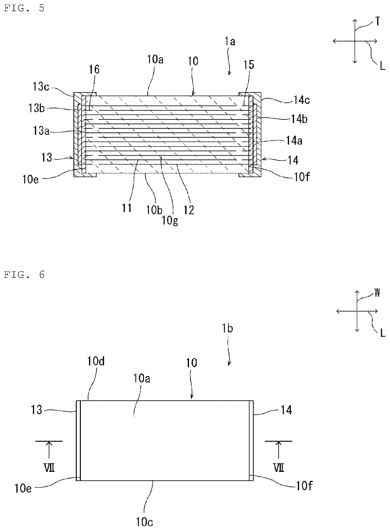
[0118]FIG. 6 is a schematic plan view of the electronic component of a third preferred embodiment of the present invention. FIG. 7 is a schematic cross-sectional view taken on line VII-VII of FIG. 6.
[0119]The electronic component 1b according to the third preferred embodiment is different from the electronic component 1 according to the first preferred embodiment in that the first external electrode 13 is defined by only the conductive layer inside which the end portion of the first internal electrode 11 positions, and the second external electrode 14 is defined by only the conductive layer inside which the end portion of the second internal electrode 12 positions. In preferred embodiments of the present invention, the first external electrode only has to have at least the conductive layer inside which the end portion of the first internal electrode or the end portion of the second auxiliary electrode positions, and the second external electrode only has to have at least the conduct...
PUM
| Property | Measurement | Unit |
|---|---|---|
| width | aaaaa | aaaaa |
| width | aaaaa | aaaaa |
| width | aaaaa | aaaaa |
Abstract
Description
Claims
Application Information
 - R&D
- Intellectual Property
- Life Sciences
- Materials
- Tech Scout
- Unparalleled Data Quality
- Higher Quality Content
- 60% Fewer Hallucinations
Browse by: Latest US Patents, China's latest patents, Technical Efficacy Thesaurus, Application Domain, Technology Topic, Popular Technical Reports.
© 2025 PatSnap. All rights reserved.Legal|Privacy policy|Modern Slavery Act Transparency Statement|Sitemap|About US| Contact US: help@patsnap.com


