Multilayer resin substrate and method of manufacturing multilayer resin substrate
a resin substrate and multi-layer technology, applied in the direction of printed circuit manufacturing, circuit bendability/stretchability, printed circuit aspects, etc., can solve the problems of difficult to apply bending stress to the conductor pattern, etc., to achieve the effect of significantly reducing or preventing the cracking or peeling of the conductor pattern, and difficult to apply bending stress
- Summary
- Abstract
- Description
- Claims
- Application Information
AI Technical Summary
Benefits of technology
Problems solved by technology
Method used
Image
Examples
first preferred embodiment
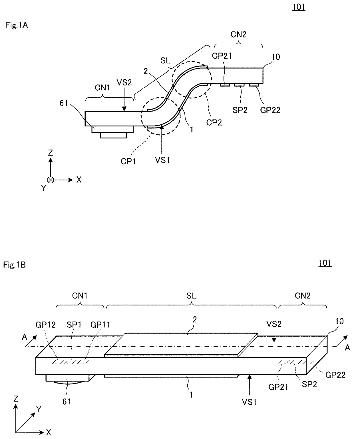
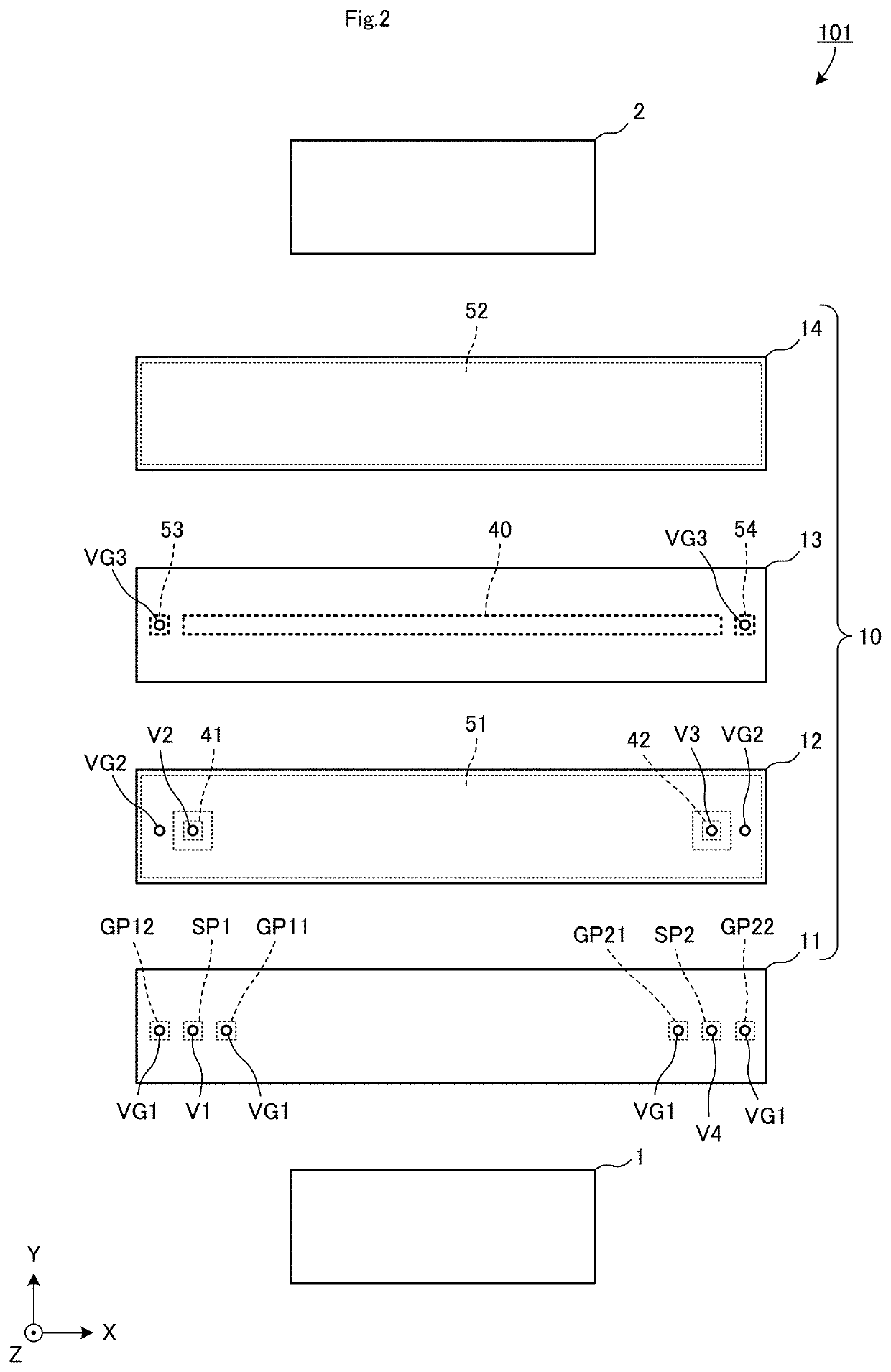
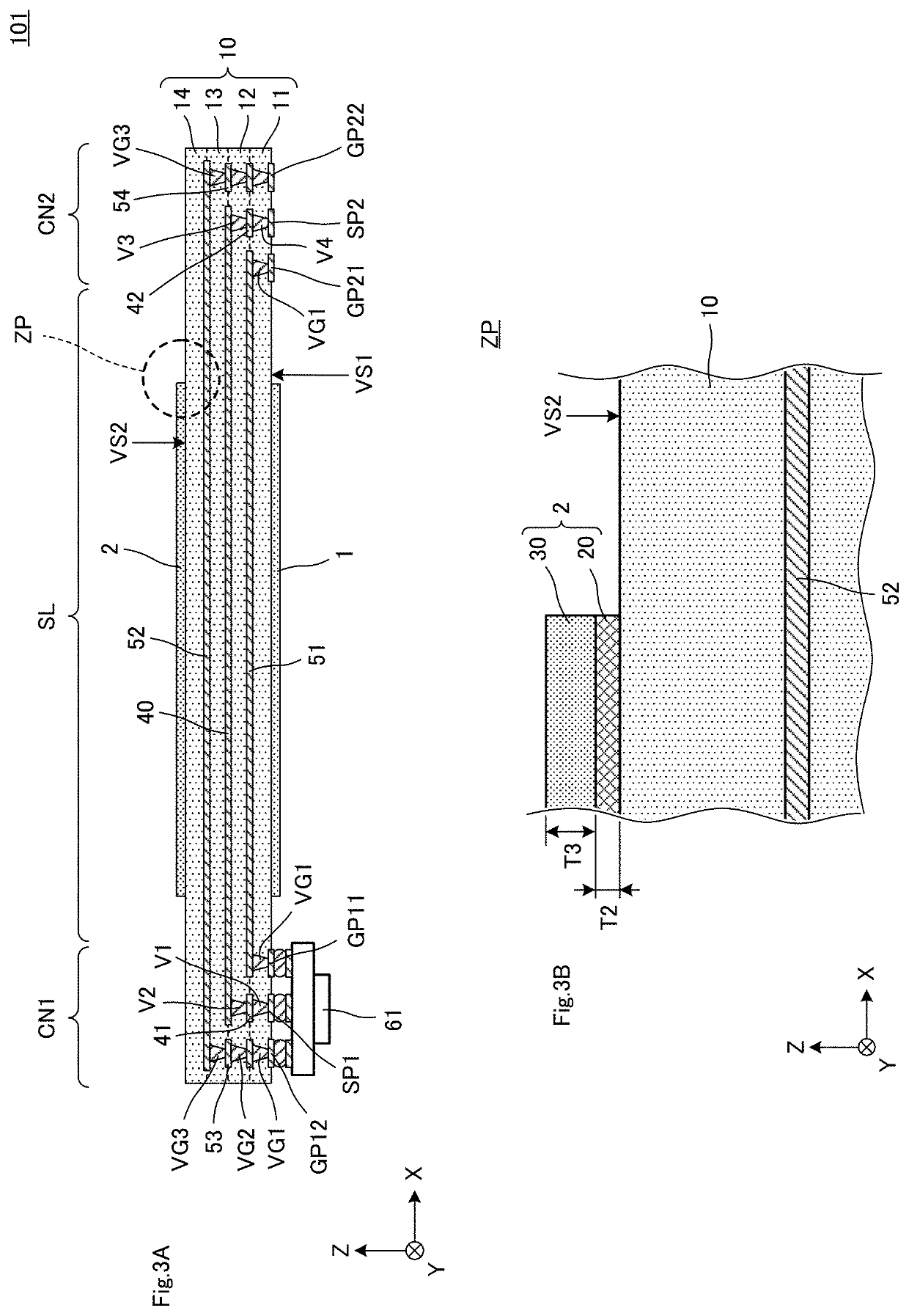
[0025]FIG. 1A is a front view of a multilayer resin substrate 101 according to a first preferred embodiment of the present invention, and FIG. 1B is an external perspective view showing a state before the multilayer resin substrate 101 is bent. FIG. 2 is an exploded plan view of the multilayer resin substrate 101. FIG. 3A is an A-A cross-sectional view in FIG. 1B, and FIG. 3B is an enlarged view of a ZP portion in FIG. 3A.
[0026]The multilayer resin substrate 101 according to the first preferred embodiment of the present invention may be a cable that connects a plurality of circuit boards to each other, for example.
[0027]The multilayer resin substrate 101 includes connection portions CN1 and CN2, and a line portion SL. The connection portions CN1 and CN2 are connected to other circuit boards. As will be described in detail later, a transmission line that connects the connection portions CN1 and CN2 is provided in the line portion SL. In the multilayer resin substrate 101, the connect...
second preferred embodiment
[0075]A second preferred embodiment of the present invention provides an example of a multilayer resin substrate in which a plurality of bent portions are provided and a protective layer is independently provided for each bent portion.
[0076]FIG. 5A is a front view of a multilayer resin substrate 102 according to the second preferred embodiment, and FIG. 5B is an external perspective view showing a state before the multilayer resin substrate 102 is bent. FIG. 6 is an exploded plan view of the multilayer resin substrate 102. FIG. 7 is a B-B cross-sectional view in FIG. 5B.
[0077]The multilayer resin substrate 102 according to the present preferred embodiment is an electronic component that is surface-mounted on a circuit board having a level difference, for example.
[0078]The multilayer resin substrate 102 is different from the multilayer resin substrate 101 according to the first preferred embodiment in that a stacked body 10A and a plurality of protective layers 1A, 1B, 2A, and 2B are...
third preferred embodiment
[0104]A third preferred embodiment of the present invention provides an example of a multilayer resin substrate in which a protective layer is provided only on the second main surface.
[0105]FIG. 9A is a front view of a multilayer resin substrate 103 according to the third preferred embodiment of the present invention, and FIG. 9B is an external perspective view showing a state before the multilayer resin substrate 103 is bent. FIG. 10 is an exploded plan view of the multilayer resin substrate 103. FIG. 11A is a C-C cross-sectional view in FIG. 9B, and FIG. 11B is a D-D cross-sectional view in FIG. 9B.
[0106]The multilayer resin substrate 103 includes a stacked body 10B, a conductor pattern (a signal conductor 40 and external connection electrode SP1 and SP2), interlayer connection conductors V1, V2, and V3, and a protective layer 2. The multilayer resin substrate 103 is different from the multilayer resin substrate 101 according to the first preferred embodiment in that the ground co...
PUM
| Property | Measurement | Unit |
|---|---|---|
| flexible | aaaaa | aaaaa |
| thickness | aaaaa | aaaaa |
| flatness | aaaaa | aaaaa |
Abstract
Description
Claims
Application Information
 - R&D
- Intellectual Property
- Life Sciences
- Materials
- Tech Scout
- Unparalleled Data Quality
- Higher Quality Content
- 60% Fewer Hallucinations
Browse by: Latest US Patents, China's latest patents, Technical Efficacy Thesaurus, Application Domain, Technology Topic, Popular Technical Reports.
© 2025 PatSnap. All rights reserved.Legal|Privacy policy|Modern Slavery Act Transparency Statement|Sitemap|About US| Contact US: help@patsnap.com


