System and method for filling vias

a technology of integrated circuits and vias, applied in the field of system and a method for filling vias, can solve the problems of additional process steps, insufficient mechanical strength to provide long-term reliability, etc., and achieve the effect of reducing the number of process steps, and reducing the manufacturing cost of products

Active Publication Date: 2010-08-24
TEXAS INSTR INC
View PDF6 Cites 0 Cited by
  • Summary
  • Abstract
  • Description
  • Claims
  • Application Information

AI Technical Summary

Benefits of technology

[0011]An advantage of an embodiment is the reduction in the number of process steps required to fill the via. The reduction in the number of process steps may reduce the manufacturing costs of the product. Furthermore, the reduction in the number of process steps may reduce the occurrence of manufacturing errors, which may increase product yield, further reducing the cost of the product.
[0012]A further advantage of an embodiment is that fewer fill materials and process steps may help increase the planarity of the via and the area immediately surrounding the via. For systems that depend on optical reflectivity of structures on the integrated circuit, such as projection display systems that use micro-displays containing filled vias, the increase in planarity may positively impact image quality.
[0013]Yet another advantage of an embodiment is the improved structural rigidity of the via with the fill, which may increase the reliability of the via functioning as a mechanical connector.

Problems solved by technology

Non-electrically conductive vias may also be created using the same techniques and materials, however, these techniques may not provide adequate mechanical strength to provide long-term reliability.
A disadvantage of the disclosed technique is the requirement of additional process steps to protect the bottom of the opening with a protective layer prior to the sputtering or etching, and then removing the protective layer after the sputtering or etching.

Method used


Image

  • System and method for filling vias
  • System and method for filling vias
  • System and method for filling vias

Examples


Embodiment Construction

[0021]The making and using of the embodiments are discussed in detail below. It should be appreciated, however, that the present invention provides many applicable inventive concepts that can be embodied in a wide variety of specific contexts. The specific embodiments discussed are merely illustrative of specific ways to make and use the invention, and do not limit the scope of the invention.

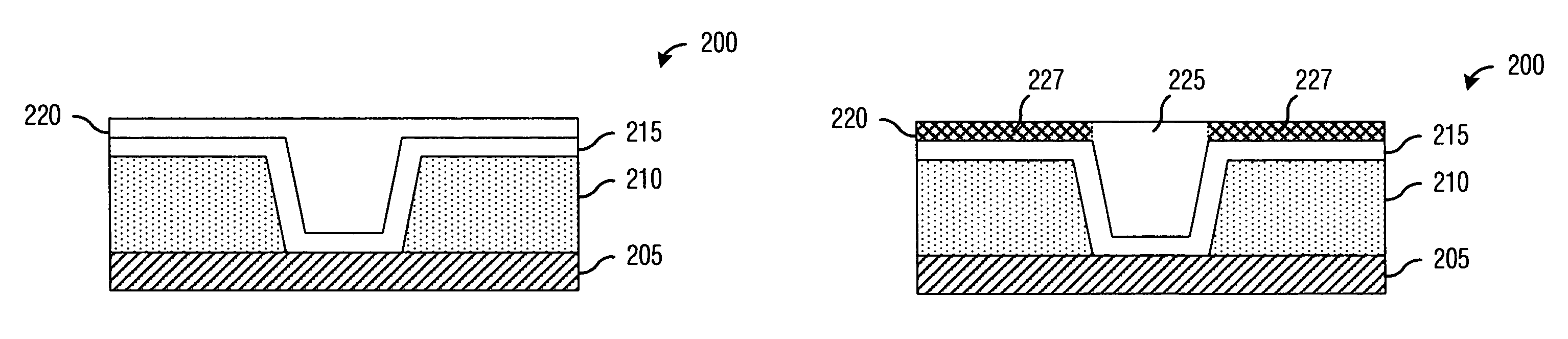
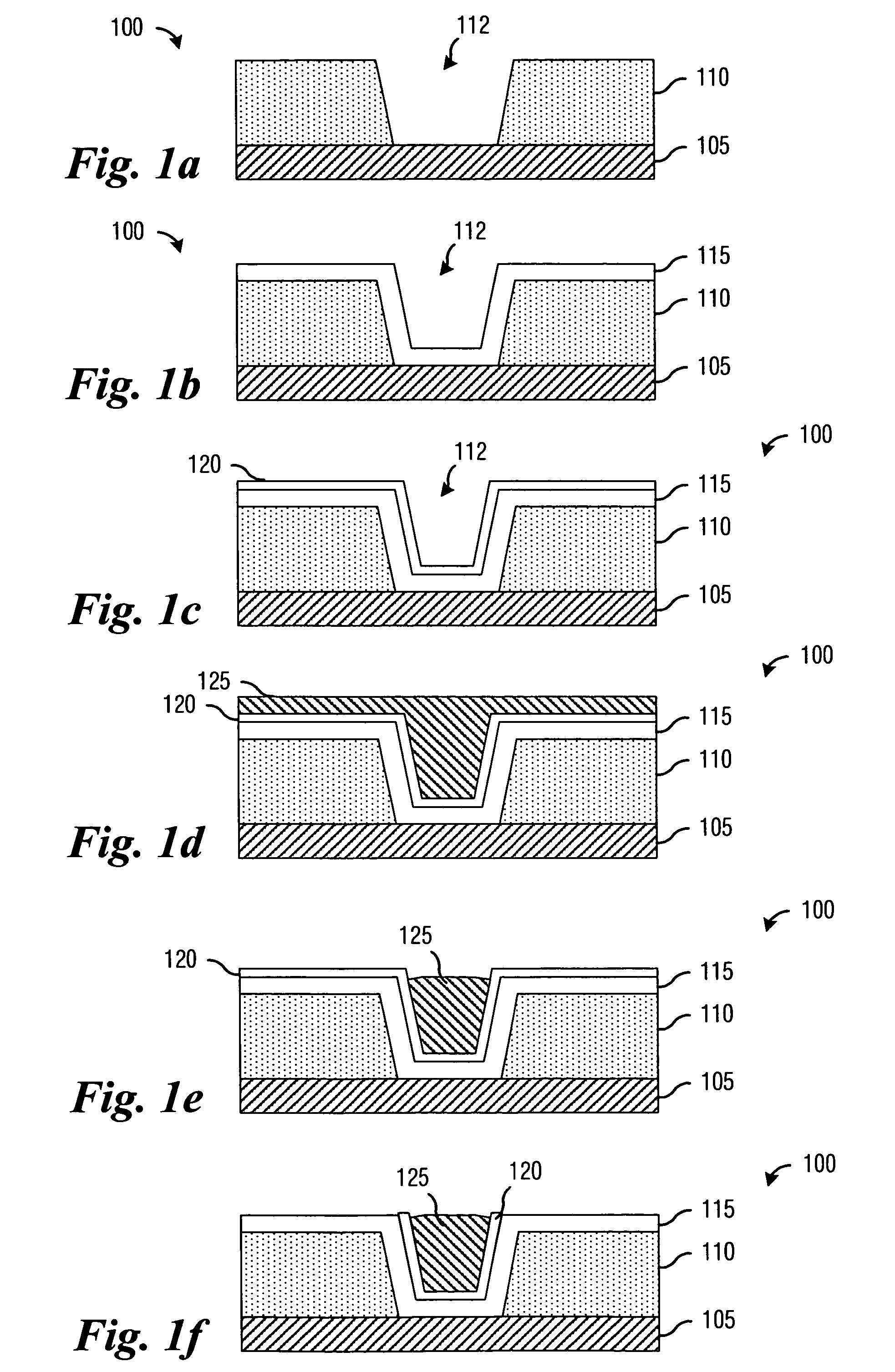
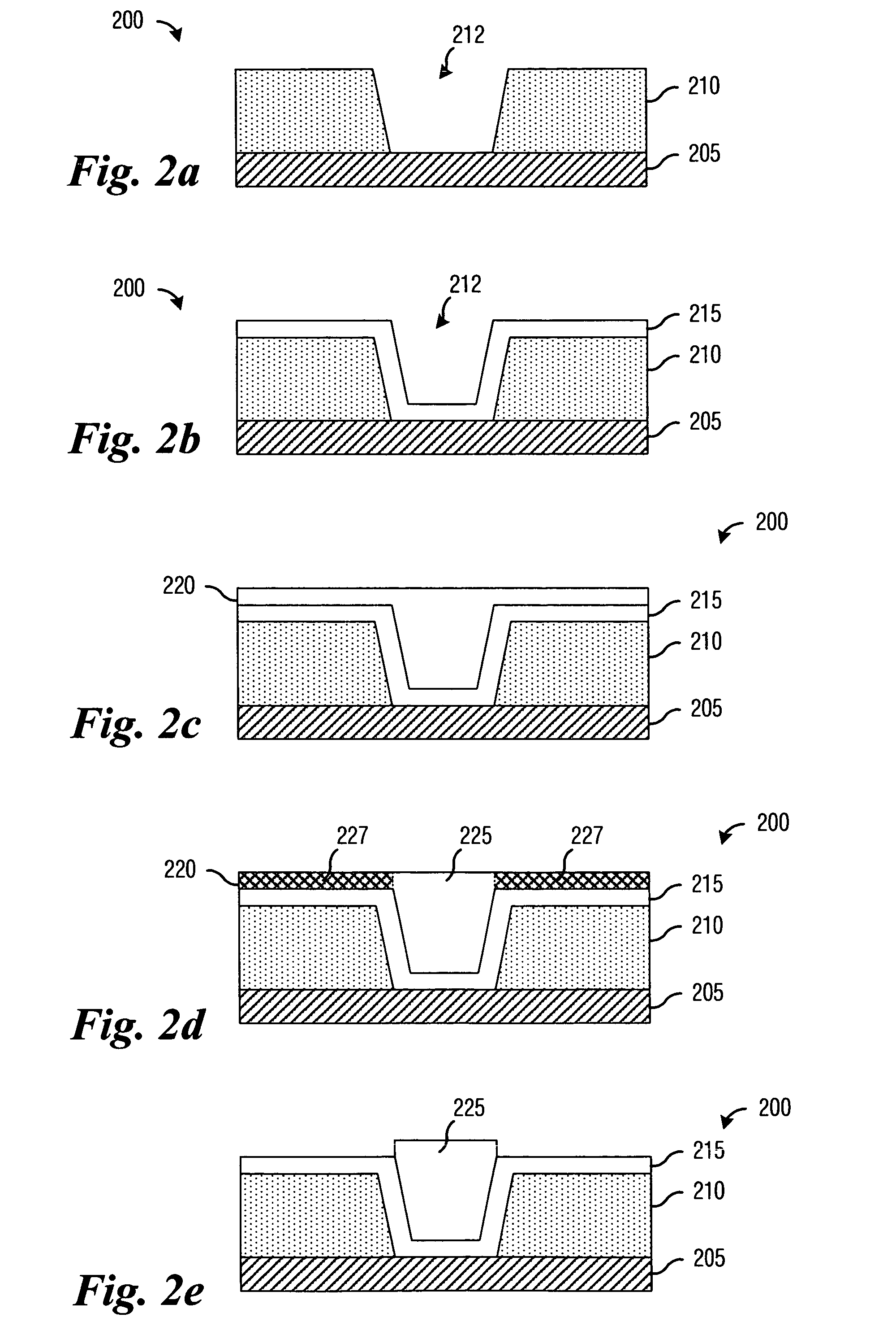
[0022]The embodiments will be described in a specific context, namely a micro-electro-mechanical system (MEMS) containing positional micromirrors (also referred to as a digital micromirror device (DMD)) that may be used as a spatial light modulator in a projection display system. The invention may also be applied, however, to other integrated circuits wherein there is a desire to fill vias to increase their structural integrity and / or planarity, regardless of whether the vias are used for electrical connectivity or mechanical connectivity.

[0023]With reference now to FIGS. 1a through 1f, there ar...


PUM


Abstract

System and method for filling vias in integrated circuits A preferred embodiment comprises forming a spacer layer on a substrate, forming a via with walls and a bottom in the spacer layer, depositing a conformal conductive layer on the spacer layer and on the walls and bottom of the via, spinning-on a photo-definable material on the conductive layer, forming a fill layer on the conductive layer and filling the via, exposing portions of the fill layer to an exposing light using a photomask, developing the fill layer to remove select portions of the fill layer and leave a portion of the fill layer filling the via, and removing the spacer layer. The use of a spin-on photo-definable material increases the material's filling and planarizing capabilities, while enabling a reduction in the number of process steps, which may reduce the likelihood of manufacturing defects, thereby increasing manufacturing yield.

Description

TECHNICAL FIELD[0001]The present invention relates generally to a system and a method for integrated circuits, and more particularly to a system and a method for filling vias in integrated circuits.BACKGROUND[0002]A via, a plated hole etched in one or more layers of an integrated circuit and used to provide a vertical connection between different layers, may be used for many different purposes. A via may provide electrical connectivity between different layers of the integrated circuit. Additionally, in a micro-electro-mechanical system (MEMS) a via may provide mechanical connectivity between structures in the integrated circuit. A via may also be used to provide both electrical and mechanical connectivity.[0003]In a digital micromirror device (DMD) based projection display system, wherein a large number of micromirrors pivot along an axis based on image data from an image being displayed, a via may be used to provide electrical connectivity between distant conductive layers and con...

Claims


Application Information

Patent Timeline
Patent Type & Authority Patents(United States)
IPC IPC(8): H01L21/44
CPCB81C1/00611B81B2203/0353B81B2207/07B81C2201/0123H01L23/5226H01L2924/0002Y10S438/947H01L2924/00
Inventor FRANKLIN, MARK ANDREWJABBOUR, GEORGINA MARIEBAKER, JAMES CARL
Owner TEXAS INSTR INC
Why Eureka
Try Eureka