
System and method for dispensing material onto a semiconductor wafer

Active Publication Date: 2010-08-31
NAT SEMICON CORP
View PDF8 Cites 2 Cited by
  • Summary
  • Abstract
  • Description
  • Claims
  • Application Information

AI Technical Summary

Problems solved by technology

One of the more expensive materials applied to the wafers is photoresist, which allows lithography to be used to etch other types of layers on the wafers.
Conventional methods for applying material to the semiconductor wafers have many disadvantages associated with them, especially for materials such as photoresist that can react with air.
Crystallization of the material caused by such reactions is a major source of debris when the material is applied to the wafers.
Eventually, the line widths may become so small that the debris may become a limiting factor.
However, although this suck-back force may reduce crystallization, it fails to eliminate crystallization as a source of debris.
In addition, conventional application methods include many other sources of debris that are unaffected by the use of a suck-back force.
Disadvantages associated with conventional application methods also include the fact that many materials, such as photoresist, are supplied in bulk containers.
As a result, any contamination renders the whole batch unusable.
Another disadvantage is that pumps typically incorporate a flexible bellows that comes in contact with the material itself, which results in another source of contamination as the material is flexed during each dispense and suck-back cycle.
Problems with incorrect volume can lead to scrap, rework and / or excess cost and disposal fees associated with the effluent material that is spun off the wafer during the thickness control (spin) function.
Disadvantages also include the use of the Teflon-type tubing line that transports the pump output up to the nozzle.
In addition, the nozzle itself may become damaged in such a way as to shed metal debris onto the wafer or may become contaminated with crystallized material.
However, there is no algorithm for determining how many dummy wafers should be used to guarantee that the debris is flushed out.
This method also results in the waste of the material that is used on the dummy wafers.
In addition, the dummy wafers must then be cleaned off or discarded, further increasing production costs.
Another disadvantage associated with conventional methods for applying material to wafers is that the material in the bulk containers may be depleted without an operator being able to determine that the material is gone.
This results in semiconductor wafers being moved along in the production line without the appropriate material being applied.

Method used


Image

  • System and method for dispensing material onto a semiconductor wafer
  • System and method for dispensing material onto a semiconductor wafer
  • System and method for dispensing material onto a semiconductor wafer

Examples


Embodiment Construction

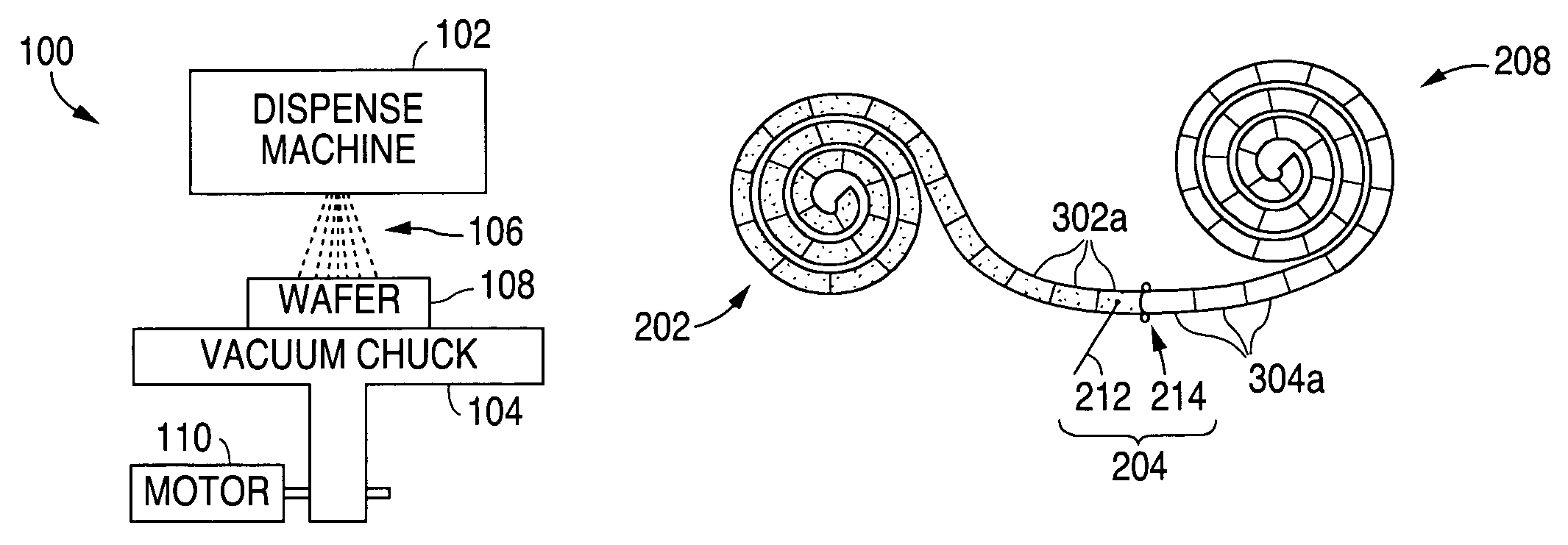
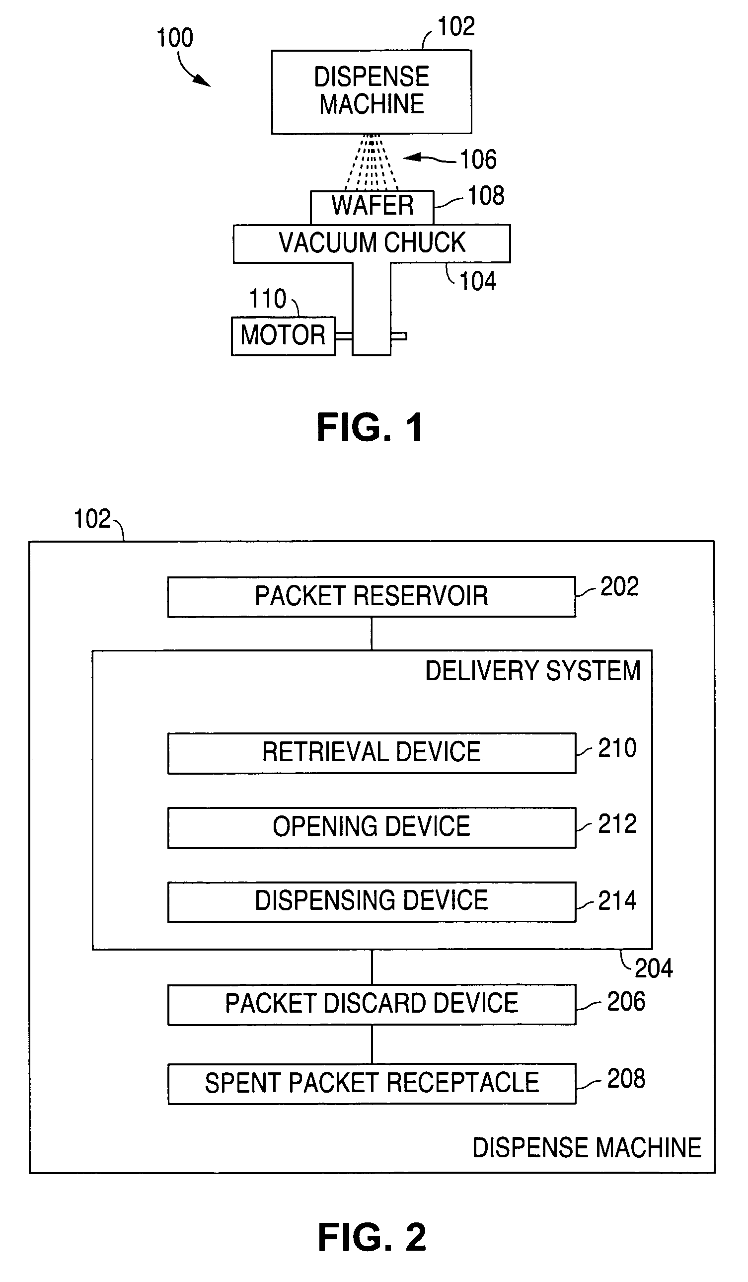
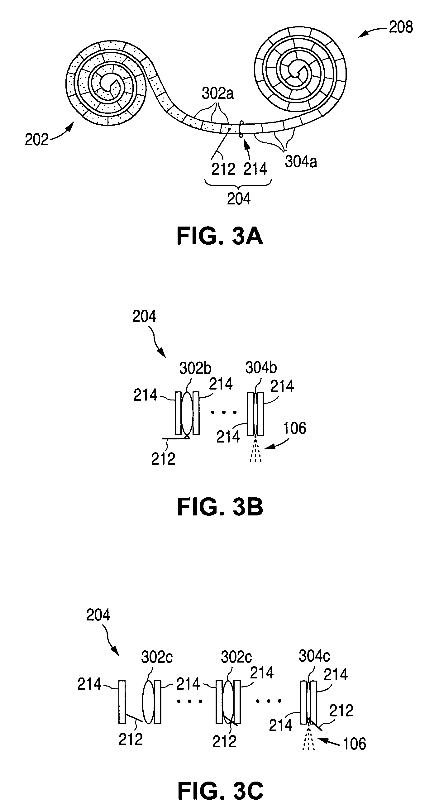
[0015]FIGS. 1 through 4, discussed below, and the various embodiments used to describe the principles of the present invention in this patent document are by way of illustration only and should not be construed in any way to limit the scope of the invention. Those skilled in the art will understand that the principles of the present invention may be implemented in any suitably arranged semiconductor fabrication system.

[0016]FIG. 1 is a block diagram illustrating a system 100 for dispensing material onto a semiconductor wafer in accordance with one embodiment of the present invention. The system 100 comprises a dispense machine 102 and a vacuum chuck 104. The dispense machine 102 is operable to dispense material 106 onto a semiconductor wafer 108. The vacuum chuck 104 is operable to hold the wafer 108 in the appropriate position while the material 106 is dispensed onto the wafer 108 by the dispense machine 102. The vacuum chuck 104 comprises a motor 110 that is operable to spin the v...


PUM


Abstract

A delivery system for dispensing material onto a semiconductor wafer is provided that includes an opening device and a dispensing device. The opening device is operable to open a packet of material. The dispensing device is operable to dispense the material from the packet onto the semiconductor wafer.

Description

TECHNICAL FIELD OF THE INVENTION[0001]The present invention relates generally to semiconductor fabrication and, more particularly, to a system and method for dispensing material onto a semiconductor wafer.BACKGROUND OF THE INVENTION[0002]The fabrication of semiconductor devices is an important part of manufacturing many consumer products, such as cell phones, personal computers and numerous other products. In fabricating the semiconductor wafers, metals, chemicals and other materials are applied to the wafers in many layers in order to generate a variety of different devices on the wafers. One of the more expensive materials applied to the wafers is photoresist, which allows lithography to be used to etch other types of layers on the wafers.[0003]Conventional methods for applying material to the semiconductor wafers have many disadvantages associated with them, especially for materials such as photoresist that can react with air. Crystallization of the material caused by such reacti...

Claims


Application Information

Patent Timeline
IPC IPC(8): B05C5/00B65D35/22B05C11/02
CPCH01L21/6715
Inventor LOGSDON, GEORGE
Owner NAT SEMICON CORP
Learn More