Programmable integrated circuit having built in test circuit

Active Publication Date: 2010-08-31
SILICON STORAGE TECHNOLOGY
View PDF3 Cites 27 Cited by
  • Summary
  • Abstract
  • Description
  • Claims
  • Application Information

AI Technical Summary

Problems solved by technology

The problem with the device 10 is that as the scale of integration increases, more and more logic elements 12 can be fabricated on a single integrated circuit die.
As the number of LUTs are placed on a singl

Method used


Image

  • Programmable integrated circuit having built in test circuit
  • Programmable integrated circuit having built in test circuit
  • Programmable integrated circuit having built in test circuit

Examples


Embodiment Construction

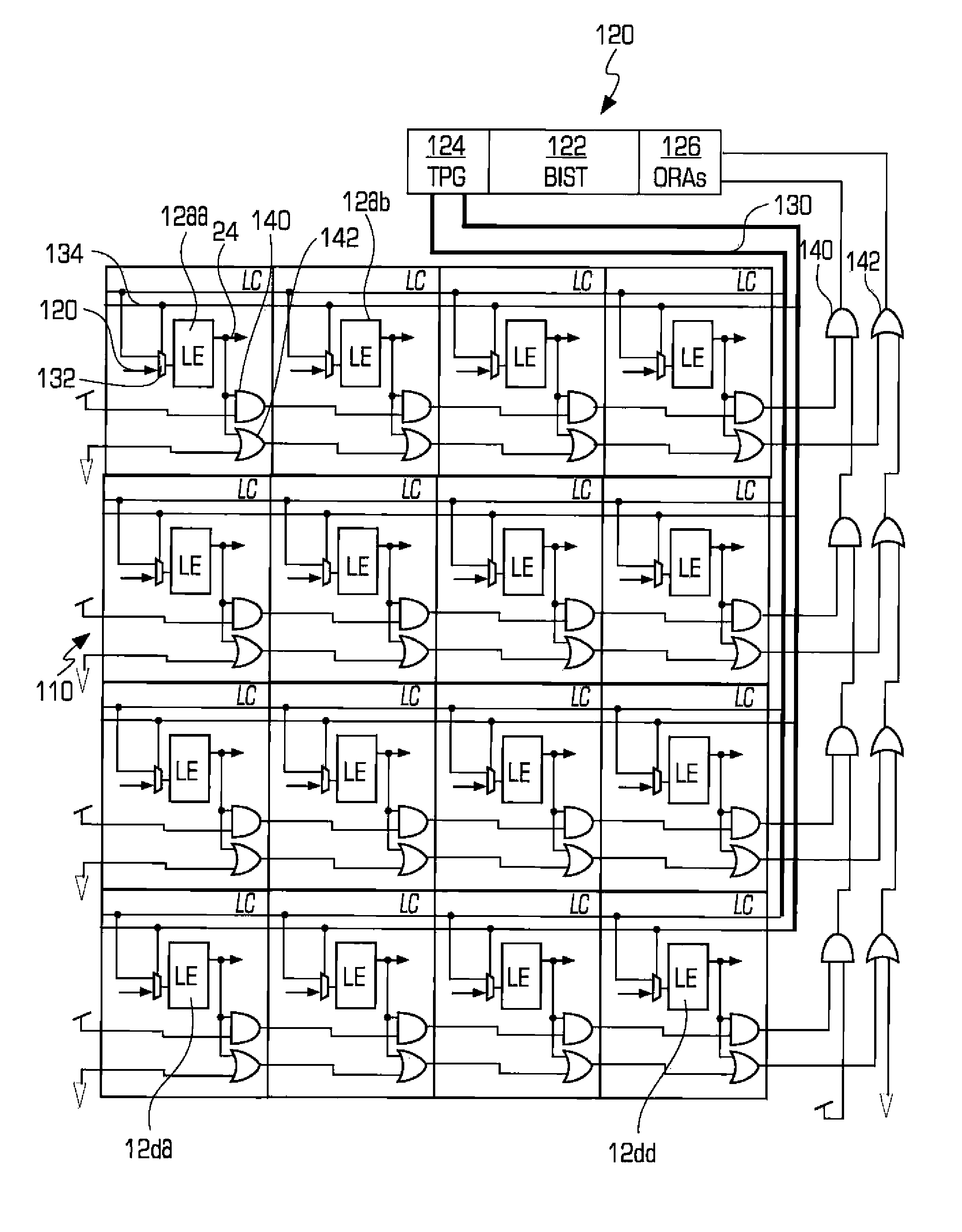
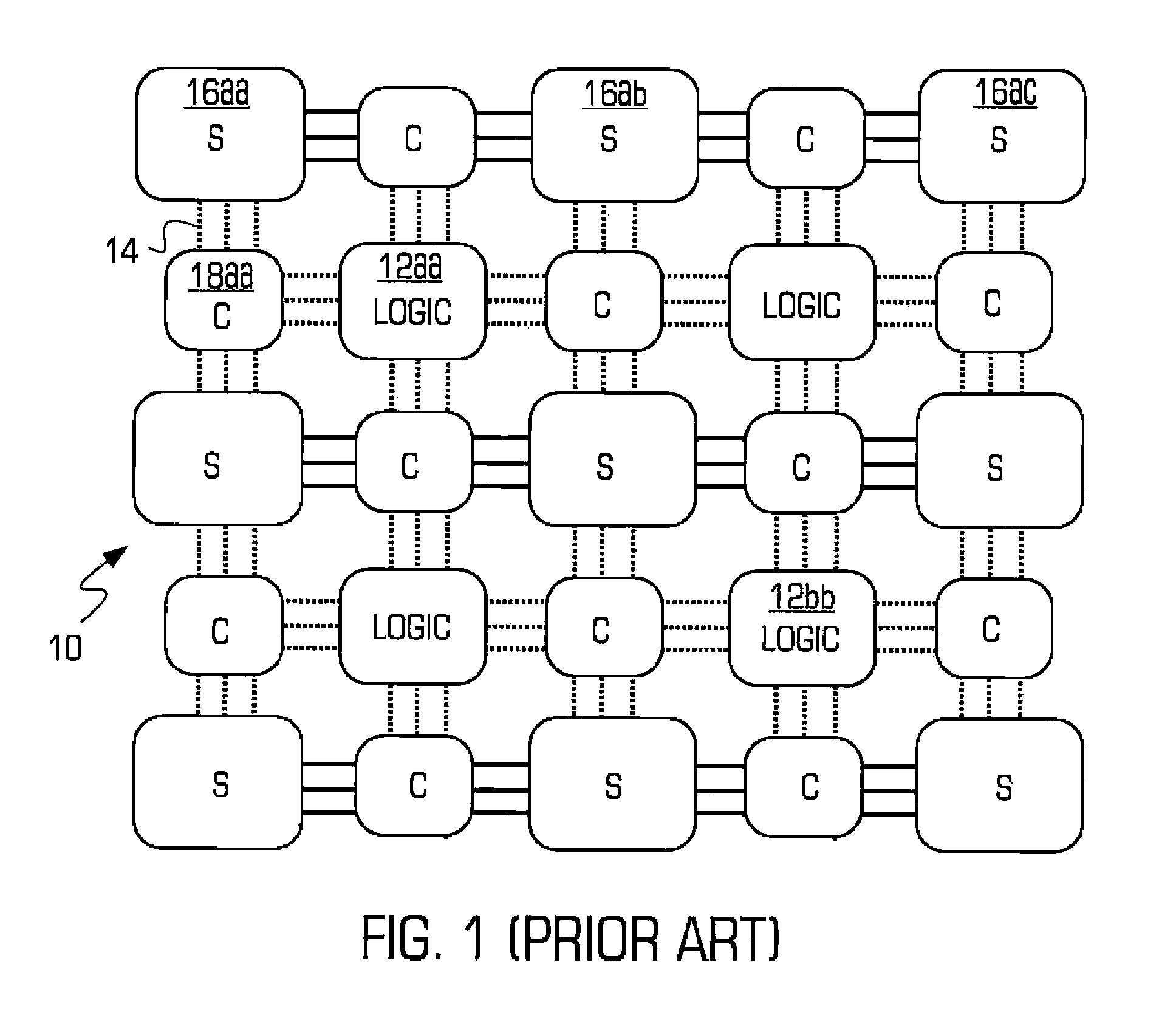
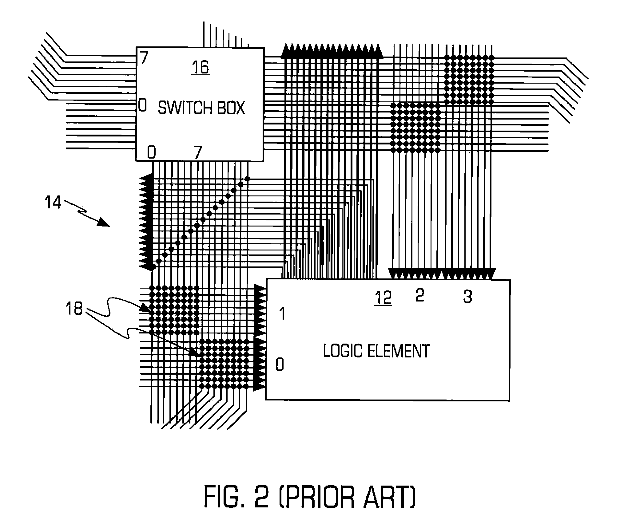
[0018]Referring to FIG. 4 there is shown a block level diagram of an integrated circuit device 110 of the present invention. The device 110 comprises an array of logic elements 12 arranged in a plurality of rows and columns. Each of the logic elements 12 can be programmed to perform a particular logic function, such as AND, OR or other logic functions. Each row of logic elements 12 is separated from one another, and each column of logic elements 12 is also separated from one another. Between the separation of the rows of logic elements 12 and the columns of logic elements 12 is a group of interconnect lines 14 (not shown). The group of interconnect lines 14 comprises a plurality of lines 14. The group of lines 14 pass through a plurality of switches 16 (not shown), which are also arranged in a plurality of rows and columns. Each of the switches 16 routes the connection of the interconnect lines from rows to columns or vice-versa. The group of interconnect lines 14 are also connected...


PUM


Abstract

A programmable integrated circuit has a plurality of logic elements with each logic element having a plurality of input leads and at least one output lead. The programmable integrated circuit further comprises a group of interconnect lines, and a first set of programmable circuits for electrically connecting the input and output leads of the plurality of logic elements to each other through the group of interconnect lines. The programmable integrated circuit further comprises a test circuit having at least one input and one output. Further the programmable integrated circuit comprises a second set of programmable circuits for electrically connecting the one output of the test circuit to the plurality of input leads of each of the plurality of logic elements and for electrically connecting the at least one output lead of each of the plurality of logic elements to the one input of the test circuit, through the group of interconnect lines.

Description

TECHNICAL FIELD[0001]The present invention relates to a programmable integrated circuit having a built in test circuit to reduce the test time of the programmable integrated circuit.BACKGROUND OF THE INVENTION[0002]Programmable integrated circuit devices are well known in the art. See for example U.S. Pat. No. Re 34,363, whose disclosure is incorporated herein by reference in its entirety. Such devices can be programmed at the factory or in the field. In the case of the latter, they can be referred to as FPGA (Field Programmable Gate Array). Typically, they comprise an array of logic elements, each of which can be programmed to perform a particular logical function. In addition, a plurality of interconnect lines surround the plurality of logic elements. Each of the logic elements may be programmably connected to the plurality of interconnect lines. In addition, the interconnect lines may be programmably routed to supply signals to different logic elements.[0003]Referring to FIG. 1 t...

Claims


Application Information

Patent Timeline
IPC IPC(8): H03K19/00H01L25/00H03K19/173
CPCG01R31/318516H03K19/17736
Inventor SYU, TSUNG-LUYEE, WILSON KAMING
Owner SILICON STORAGE TECHNOLOGY
Why Eureka
Try Eureka