Systems for programmable chip enable and chip address in semiconductor memory

a technology of semiconductor memory and programmable chips, applied in the field of integrated circuit technology, can solve the problems of defective memory array peripheral circuitry, defective memory array memory peripheral circuitry, and defective components of semiconductor memory devices

Active Publication Date: 2009-01-13
SANDISK TECH LLC
View PDF25 Cites 27 Cited by
  • Summary
  • Abstract
  • Description
  • Claims
  • Application Information

AI Technical Summary

Problems solved by technology

As with most storage devices, semiconductor memory devices may have defective components or storage areas.
For example, the individual storage elements or memory cells of a semiconductor memory array may be defective.
Additionally, the peripheral circuitry for the memory array, including word lines, bit lines, decoders, etc., may be defective, rendering associated storage elements defective as well.
It is inevitable in any commercially fabricated semiconductor memory device that some portion of the memory array will be defective.
For instance, the number of defective memory cells of the array may exceed the redundancy capacity for the die or certain peripheral circuitry may fail, causing the die to be unusable.
When this occurs, the entire memory package containing the defective die is generally unusable and rejected 20, resulting in yield losses for the manufacturing process.
If the memory package contains multiple memory chips, the failure of a single die will result in a discarded package.

Method used


Image

  • Systems for programmable chip enable and chip address in semiconductor memory
  • Systems for programmable chip enable and chip address in semiconductor memory
  • Systems for programmable chip enable and chip address in semiconductor memory

Examples


Embodiment Construction

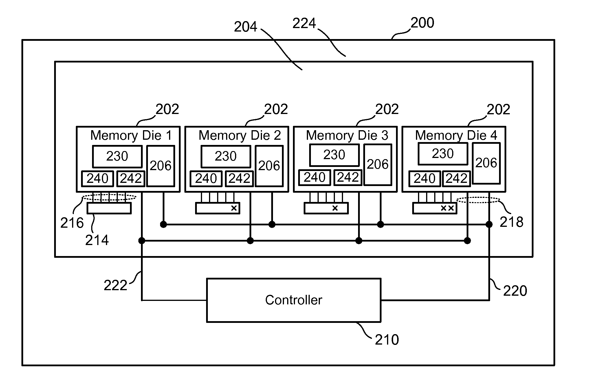
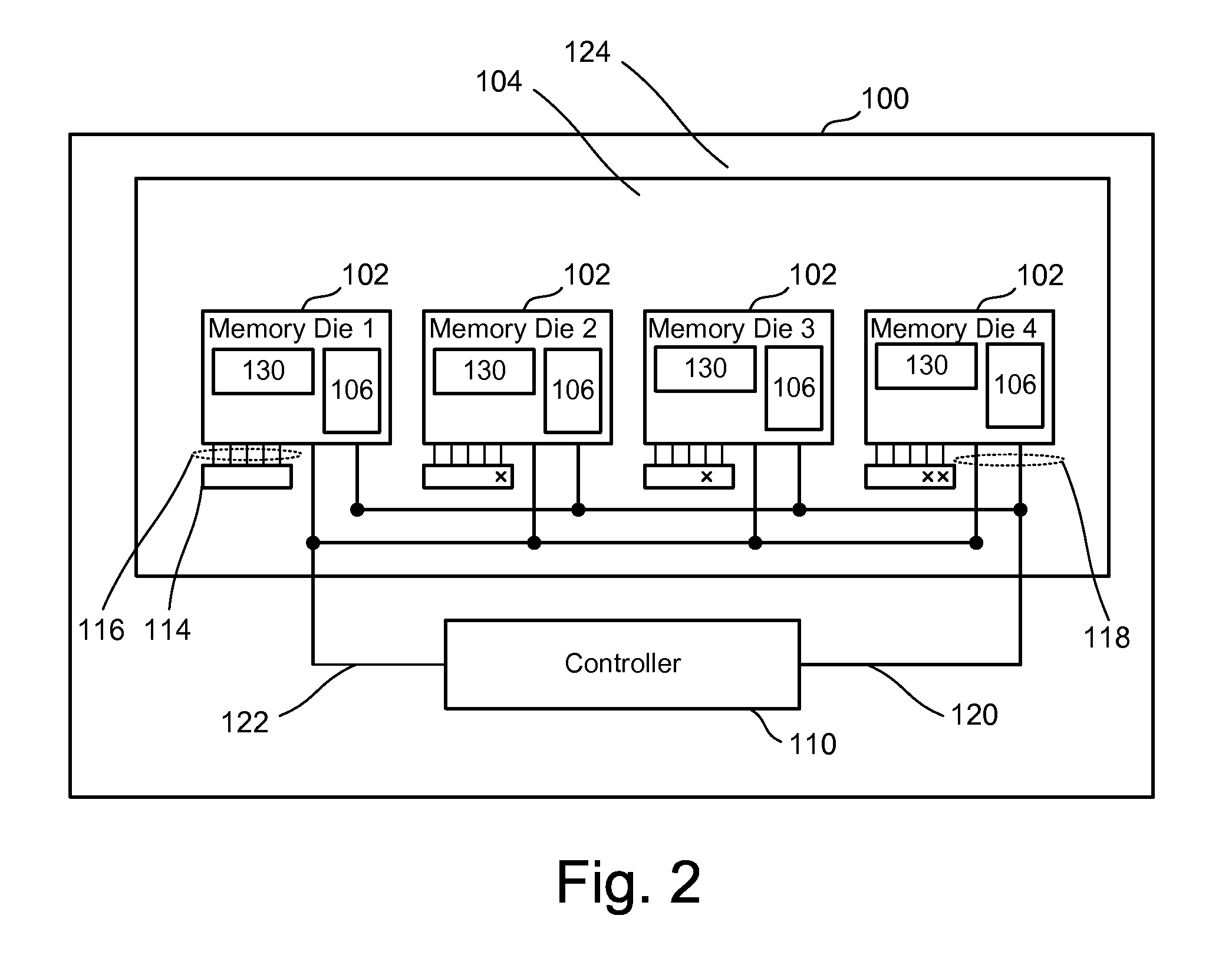
[0034]FIG. 2 schematically illustrates a non-volatile memory system 100 having a number of individual memory die 102 and a controller 110. Each memory die is an integrated circuit memory chip or die mounted on a substrate or printed circuit board 104. The controller 110 is also an integrated circuit chip or die mounted on its own printed circuit board 124. The two printed circuit boards can be mounted to a third printed circuit board (not illustrated). In other implementations, the controller and memory die may be mounted on the same board.

[0035]Each memory device includes a non-volatile memory array 106 formed of individual non-volatile memory cells. The memory array can include, but is not limited to, flash memory cells arranged using architectures such as the NAND and NOR architectures. The memory die 102 each include peripheral circuitry for addressing and controlling their respective memory array. The controller 110 is included in the memory system to control memory operations ...


PUM


Abstract

Memory die are provided with programmable chip enable circuitry to allow particular memory die to be disabled after packaging and / or programmable chip address circuitry to allow particular memory die to be readdressed after being packaged. In a multi-chip memory package, a memory die that fails package-level testing can be disabled and isolated from the memory package by a programmable circuit that overrides the master chip enable signal received from the controller or host device. To provide a continuous address range, one or more of the non-defective memory die can be re-addressed using another programmable circuit that replaces the unique chip address provided by the pad bonding. Memory chips can also be also be readdressed after packaging independently of detecting a failed memory die.

Description

CROSS-REFERENCE TO RELATED APPLICATIONS[0001]The following application is cross-referenced and incorporated by reference herein in its entirety:[0002]U.S. patent application Ser. No. 11 / 763,287, entitled “Programmable Chip Enable and Chip Address in Semiconductor Memory,” by Loc Tu, et al., filed concurrently.BACKGROUND OF THE INVENTION[0003]1. Field of the Invention[0004]The present disclosure relates to technology for fabricating integrated circuits such as semiconductor-based memory devices.[0005]2. Description of the Related Art[0006]Semiconductor-based memory, including volatile memory such as dynamic or static random access memory and non-volatile memory such as flash memory have become more popular for use in various electronic devices. For example, non-volatile semiconductor memory is used in cellular telephones, digital cameras, personal digital assistants, mobile computing devices, non-mobile computing devices and other devices. Electrically Erasable Programmable Read Only...

Claims


Application Information

Patent Timeline
Patent Type & Authority Patents(United States)
IPC IPC(8): G11C16/04
CPCG11C29/88G11C5/04
Inventor TU, LOCCHEN, JIANMAK, ALEXKUO, TIEN-CHIENPHAM, LONG
Owner SANDISK TECH LLC
Why Eureka
Try Eureka