Method of modeling and employing the CMOS gate slew and output load dependent pin capacitance during timing analysis

a technology of cmos gate and slew, applied in the field of design automation, can solve the problems of significant interconnect resistive parasitics, significant input-output errors, and approximating interconnect load by lumped capacitance susceptible to errors, and achieve the effect of high-quality models

Inactive Publication Date: 2010-08-31
GLOBALFOUNDRIES INC
View PDF10 Cites 12 Cited by
  • Summary
  • Abstract
  • Description
  • Claims
  • Application Information

AI Technical Summary

Problems solved by technology

For instance, a first reduced order model can be analyzed very fast, but it may introduce significant errors in the input-output behavior of the system.
However, in very deep sub-micron (VDSM) technologies, the effect of interconnect resistive parasitics is significant and render approximating the interconnect load by a lumped capacitance susceptible to error.
A typical conventional STA has a linear run-time complexity with respect to the number of the gates in the design.
Many model assumptions which have been made in 90+ nm nodes are no longer valid.
Constant pin capacitance models no longer accurately describe the pin's loading contribution to the total load as seen by the source terminal of the interconnect network.

Method used


Image

  • Method of modeling and employing the CMOS gate slew and output load dependent pin capacitance during timing analysis
  • Method of modeling and employing the CMOS gate slew and output load dependent pin capacitance during timing analysis
  • Method of modeling and employing the CMOS gate slew and output load dependent pin capacitance during timing analysis

Examples


Embodiment Construction

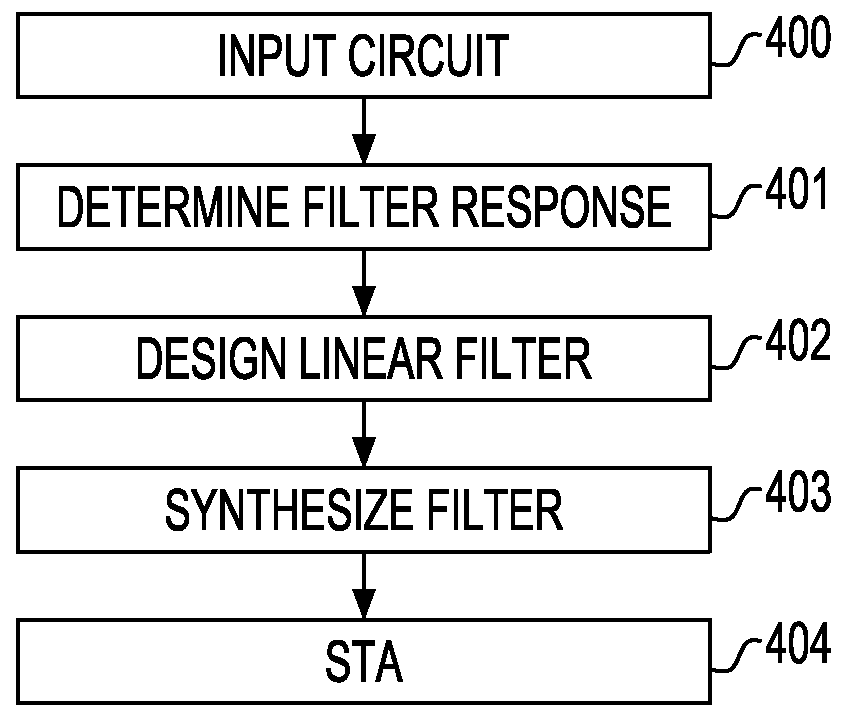
[0027]The present invention and the various features and advantageous details thereof are explained more fully with reference to the non-limiting embodiments that are illustrated in the accompanying drawings and detailed in the following description. Descriptions of well-known components and processing techniques are omitted so as to not unnecessarily obscure the present invention in detail.

Problem Statement

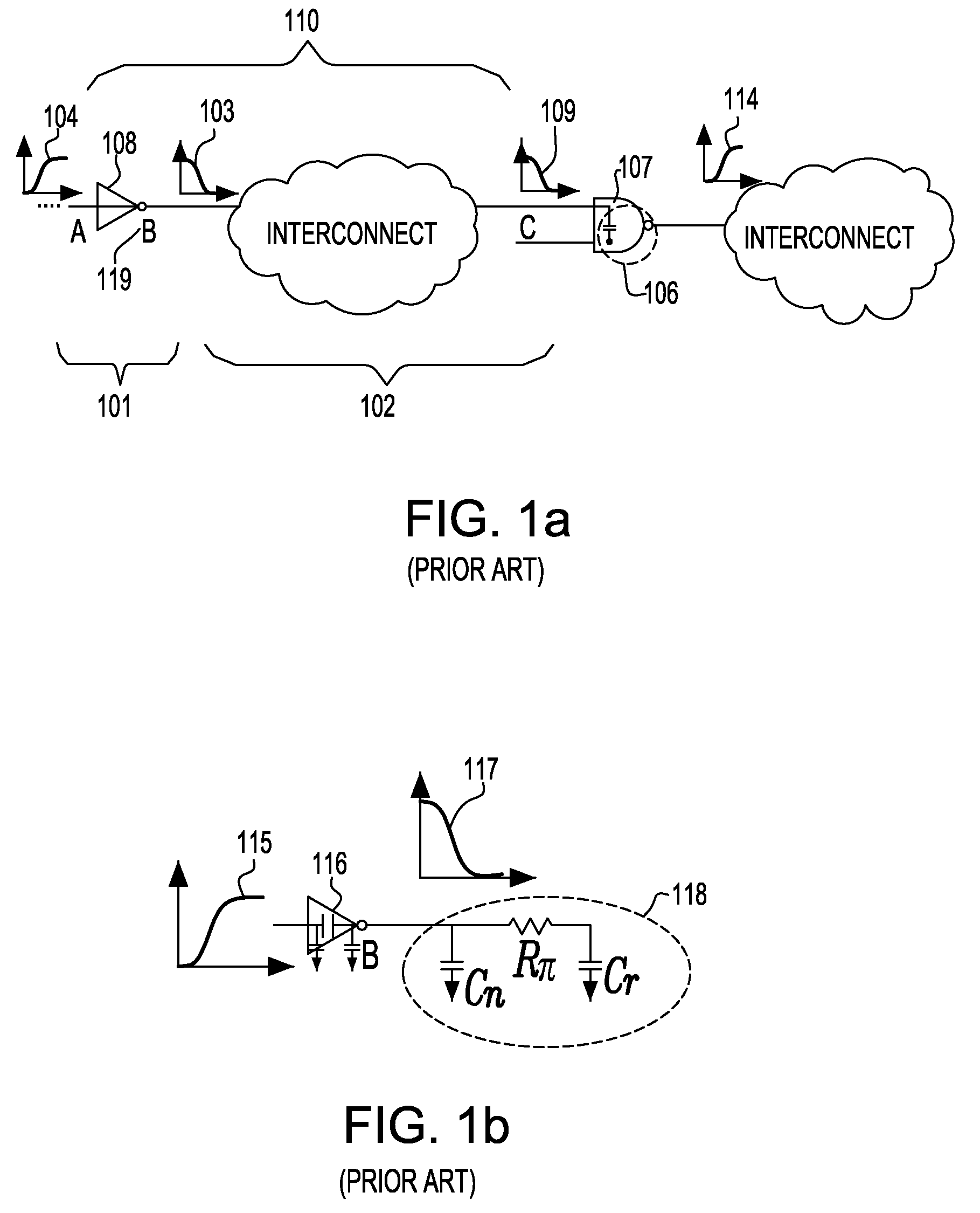
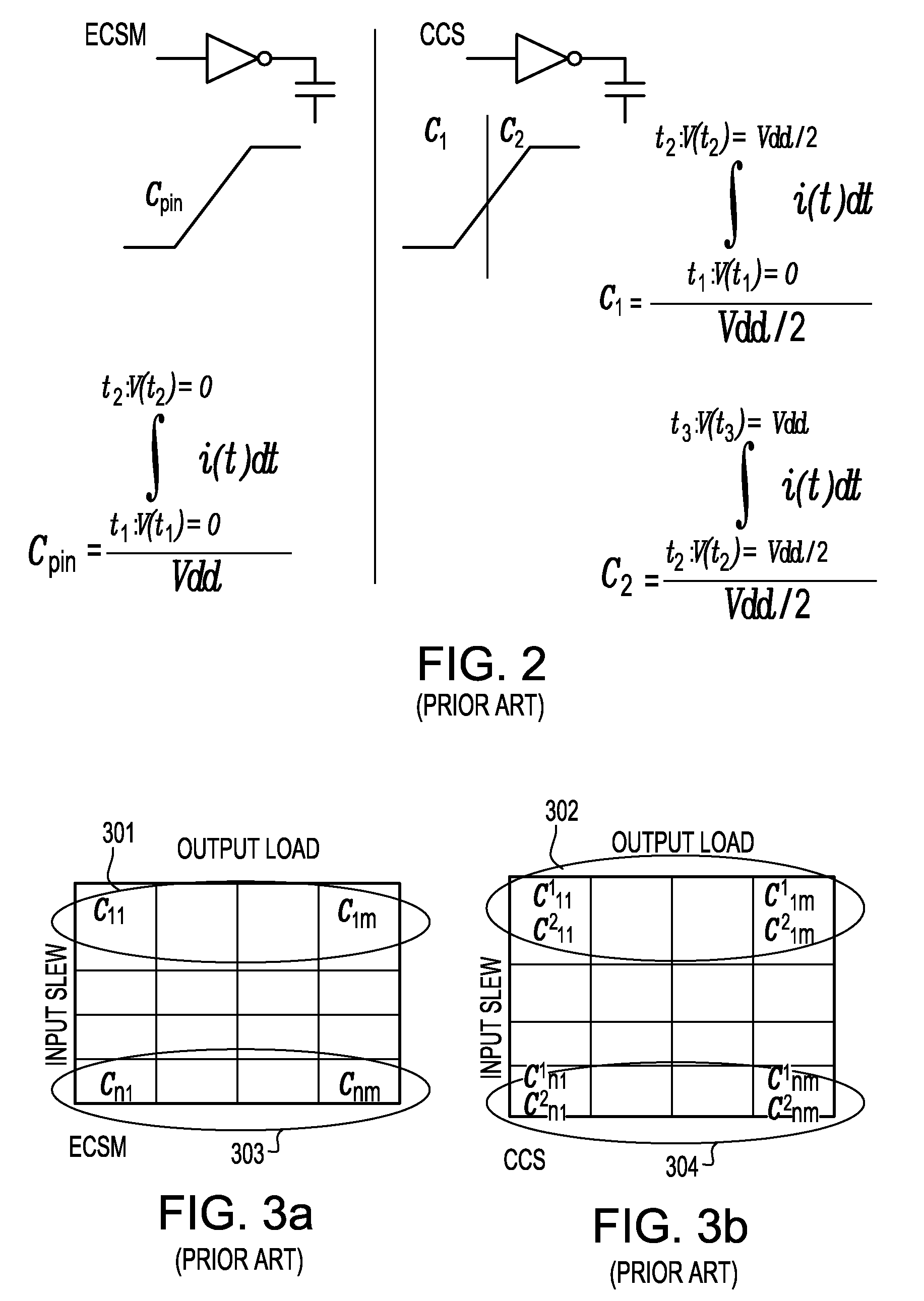
[0028]Referring back to prior art FIGS. 1a-1b, the delay 101 of a CMOS gate 108 depends on the loading at the output pin 119 of the CMOS gate. The gate input-pin capacitance 106 at each sink of the interconnect network connected to the pin 119 is required to obtain this loading. In the case of a constant pin capacitance, this capacitance is advantageously used to compute the effective loading of the net between 119 and 106. However, in the case of a slew and output load dependant pin capacitance, the input pin capacitance at pin 106 of the fan-out gate 107 requires the transition...


PUM


Abstract

An accurate method to compute the capacitance at a pin whose capacitance is slew dependant. The method uses existing library characterized data and provides an equation based approach which can easily be integrated in static timing analysis without the added resource needs that an iterative approach would require. An RC / RLC network from slew and output load dependent pin capacitance tables is generated. The resulting linear network which models the pin capacitance is then stitched to the original interconnect network and used to calculate the propagation delay across a gate and corresponding interconnect. The method steps include: a) determining a response of the gate pin capacitance to its input slew and output load; b) synthesizing a linear time-invariant filter that matches the response; c) extending the interconnect model to include the synthesized time-invariant filter; and d) inputting the extended interconnect model into a static timing analysis for determining timing behavior between a gate input and each of its fan-out gates.

Description

FIELD OF THE INVENTION[0001]This invention generally relates to the field of Design Automation of Very Large Scale Integration (VLSI) circuits, and more particularly, to the modeling and analysis of slew and load dependent input pin capacitances of metal oxide semiconductor (MOS) gates.BACKGROUND OF THE INVENTION[0002]Static timing analysis (STA) is a key step in the design of high speed very large scale integrated (VLSI) circuits. STA is used to verify that a VLSI chip performs correctly at the required frequency before it is released to manufacturing. STA typically consists of the following main steps: 1) Delay calculation, which involves modeling and calculating path delays for the gates and interconnects contained in the design, 2) Propagation of arrival, required arrival times and slews, and 3) Slack calculation for the paths in the design.[0003]Referring to FIG. 1a, there is shown a conventional overall delay from input pin A of the CMOS inverter 108 to the input pin C of the ...

Claims


Application Information

Patent Timeline
Patent Type & Authority Patents(United States)
IPC IPC(8): G06F17/50
CPCG06F17/5031G06F30/3312
Inventor BHANJI, ADILABBASPOUR, SOROUSHFELDMANN, PETERSINHA, DEBJIT
Owner GLOBALFOUNDRIES INC
Why Eureka
Try Eureka