Method of underfill air vent for flipchip BGA

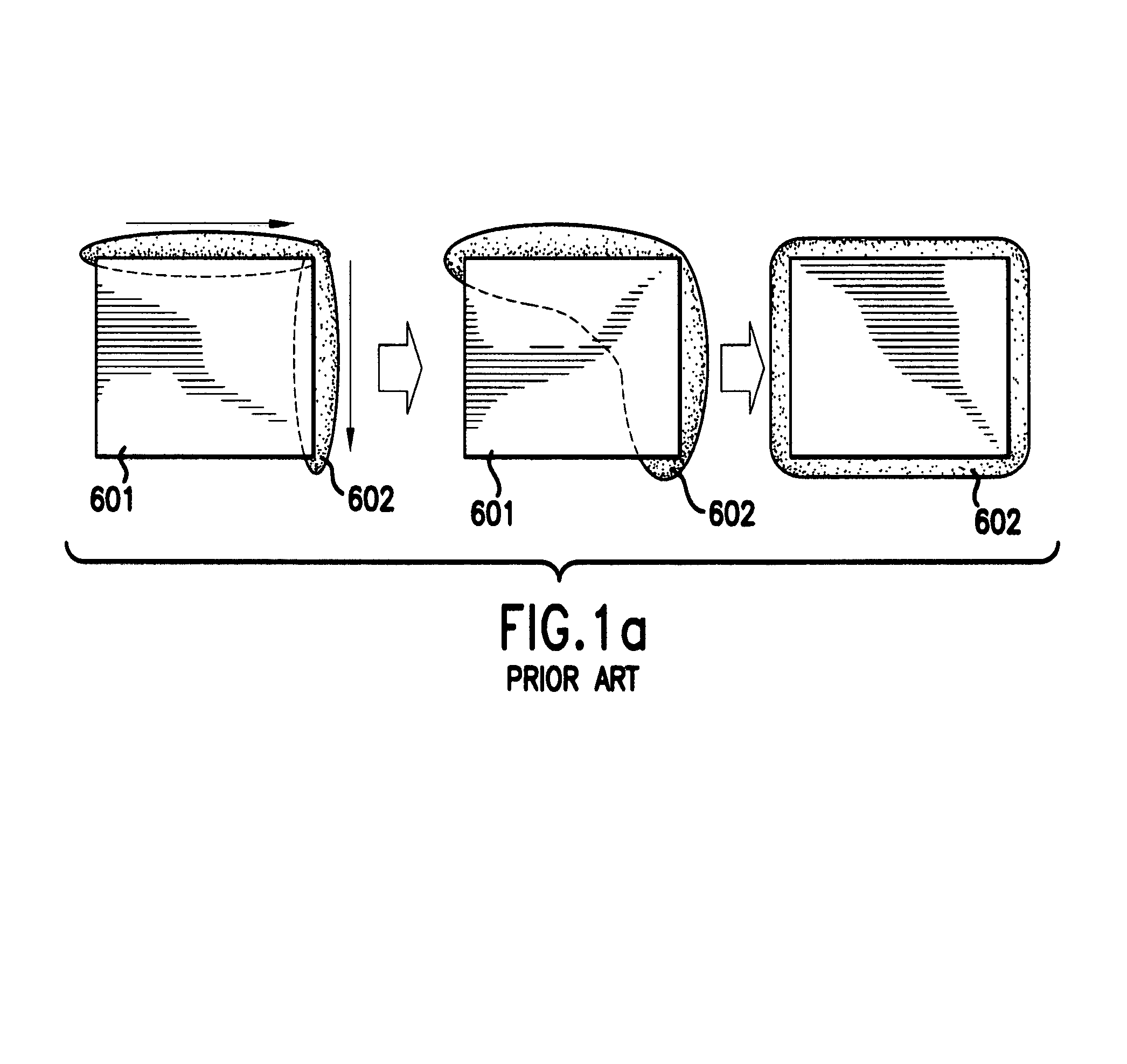
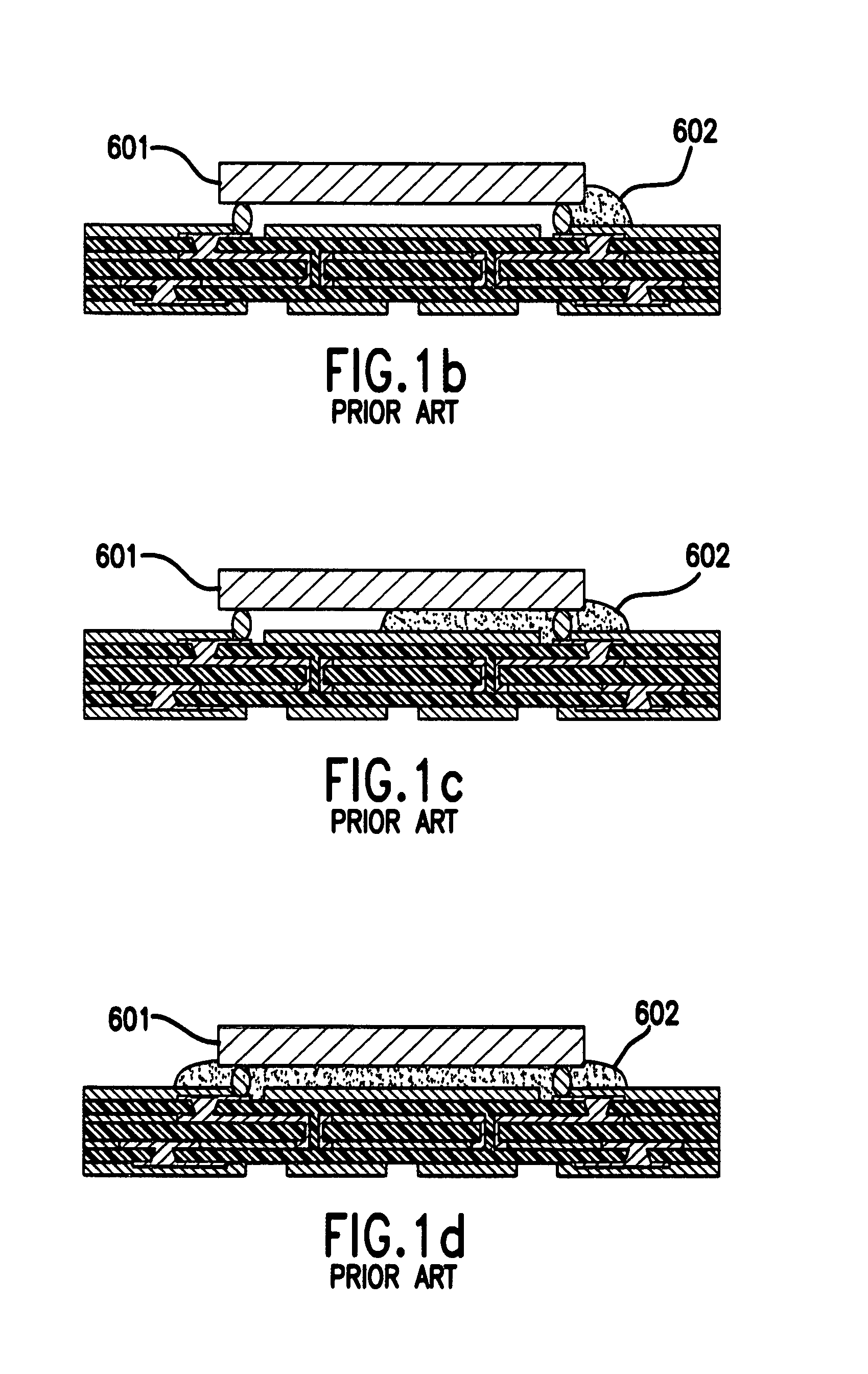
a technology of flipchip ball and air vent, which is applied in the direction of semiconductor devices, line/current collector details, semiconductor/solid-state device details, etc., can solve the problems of long processing time for the underfill resin to level out, the underfill process is not easy to control the void (i.e. air pockets or bubbles) on the semiconductor surface, and the prior art inventions do not solve the problem. , to achieve the effect of reducing the influence of the protrusion

Inactive Publication Date: 2010-09-07
GLOBALFOUNDRIES INC
View PDF9 Cites 8 Cited by
  • Summary
  • Abstract
  • Description
  • Claims
  • Application Information

AI Technical Summary

Benefits of technology

[0014]Vacuum suction is applied from the bottom side of the laminate via the through hole in order to assist the resin underfilling process. The vacuum suction is equipped at the stage which contacts the back side of the laminate. This enables faster underfilling to occur. Intentionally exposing excessive underfill resin at a rate of approximately at most 10% of the total underfill resin amount at the through hole aids in completely eliminating the occurrence of voids.
[0017]An aspect of an embodiment of the invention provides for vacuum suction and flattening excessive resin protrusions at the air vented through hole reducing voids in the underfill process.
[0018]A further aspect of an embodiment of the invention is to control excessive resin enabling reduction of droplets of underfill resin at the chip edge.
[0019]An aspect of an embodiment of the invention, though excessive underfill resins at the through hole can result in large protrusions which affect manufacturability of the apparatus and method, provides for the possibility of minimizing influences of the protrusions by flattening the underfill protrusions.

Problems solved by technology

However, the coverage of the voids (i.e. air pockets or bubbles) on the semiconductor surface is not easy to control.
Further, there is a long processing time for the underfill resin to level out.
Further, there is a significant problem created when overfill occurs absent a clean up mechanism to prevent over-spreading of the underfill material.
However, Akram et al. is not directed towards providing a laminate through hole in physical communication with an air vent and a vacuum source to promoting flow of underfill from each edge of a semiconductor chip simultaneously.
However, DiStefano et al. is not directed towards providing a laminate through hole in physical communication with an air vent and a vacuum source to promoting flow of underfill from each edge of a semiconductor chip simultaneously.
However, Hong et al. is not directed towards providing a laminate through hole in physical communication with an air vent and a vacuum source to promoting flow of underfill from each edge of a semiconductor chip simultaneously.
Further, none of the prior art inventions resolve the issue of preventing over spreading of the underfill material.
However, each of these solutions encounters significant problems.
One problem is the residual void occurring in underfill resin is not eliminated in a low cost manner.
The difficulty in the void control contributes to a significant increase in manufacturing costs in light of the prior art.
Another problem is there is a long process time for resin leveling.
Further, the inefficient and time-consuming prior art underfill techniques also cause undue and significant increases in the manufacturing costs.
None of the prior an attempts resolve the problem caused by excessive resin underfill.

Method used


Image

  • Method of underfill air vent for flipchip BGA
  • Method of underfill air vent for flipchip BGA
  • Method of underfill air vent for flipchip BGA

Examples


Embodiment Construction

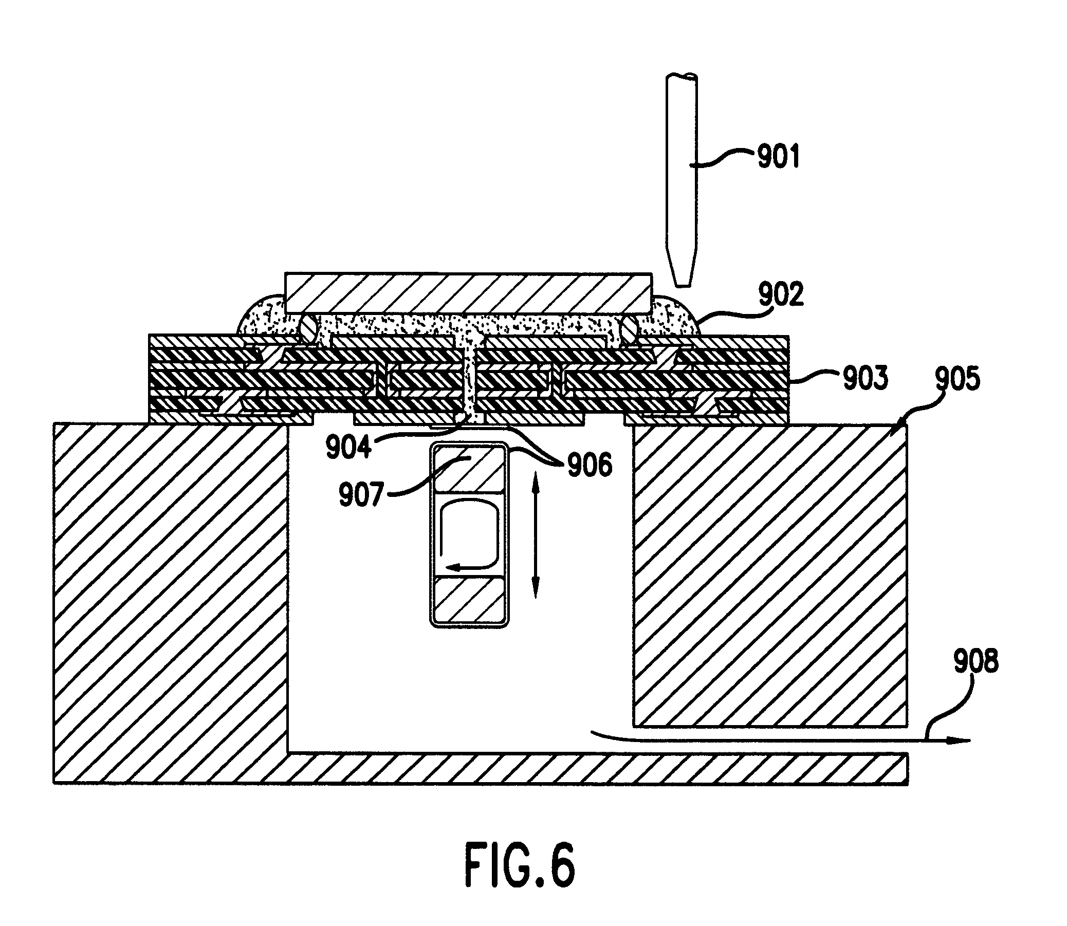
[0030]FIGS. 2a-2g illustrate an example of a flip-chip joint. FIG. 2a illustrates a wafer bumping by plating, printing, ball bonding, or the like. The bump can be comprised of solder, Cu pillar and solder, gold, or the like. The bump layout can be either peripheral or an array matrix. FIG. 2b illustrates application of a flux to the printed circuit board (PBC) which can be comprised of an organic carrier wherein no pre-solder is required. The land for the flip chip joint can be pre-soldered or the land can be comprised of Cu with anti-oxidation, or can be Ni / Au plated, etc. FIG. 2c illustrates flip chip placement. FIG. 2d illustrates reflow soldering after flip-chip placement. FIG. 2e illustrates a plasma treatment process. FIG. 2f illustrates applying an underfill resin. FIG. 2g illustrates curing the underfill resin. Each of these figures when taken as a whole illustrate the semiconductor packaging process upon which this present invention is based.

[0031]FIG. 3a illustrates a top ...


PUM

PropertyMeasurementUnit
semiconductoraaaaaaaaaa
timeaaaaaaaaaa
processing timeaaaaaaaaaa

Abstract

This invention relates to ejecting an underfill resin at multiple semiconductor die edges such that vacuum suction provided at a laminate through hole located beneath a stage enables spread of underfill resin from each edge simultaneously for quicker spread and reduction of voids. The excess underfill resin intentionally suctioned through the through hole air vent on the underside of the laminate is attracted to re-usable tape. The attracted underfill resin is cleaned from a rotating head mechanism by a cleaning pad positioned beneath a lower surface of the head.

Description

CROSS REFERENCE TO RELATED APPLICATIONS[0001]There are no cross-references related to this application.FIELD OF THE INVENTION[0002]The present invention relates to flip-chip ball grid array (BGA) packaging, and more particularly to an underfill material injection system for a semiconductor package that eliminates voids or air bubbles between a semiconductor chip and a BGA substrate during an underfill process and in a manner which shortens the underfill time.BACKGROUND OF THE INVENTION[0003]FIGS. 1a through 1d illustrate an existing technique for putting underfill resin 602 beneath the surface of a semiconductor die 601. The underfill resin 602 is placed along two adjacent edges of the semiconductor die 601 wherein the adjacent edges intersect. After a period of time has elapsed, the underfill resin 602 begins to spread by capillary effect across the under surface of the die to opposing intersecting edges until the underneath of the die is completely covered. However, the coverage o...

Claims


Application Information

Patent Timeline
Patent Type & Authority Patents(United States)
IPC IPC(8): H01L23/48
CPCH01L21/563H01L24/27H01L24/743Y10T29/49171H01L2924/01078H01L2924/01079H01L2224/16225H01L2224/32225H01L2224/73204H01L2924/15151H01L2224/73203Y10T29/49172H01L2924/01029H01L2924/00H01L2224/16237
Inventor HISADA, TAKASHINISHI, SAYAKA
Owner GLOBALFOUNDRIES INC
Why Eureka
Try Eureka