Semiconductor transistor with P type re-grown channel layer

a technology of regrown channel layer and semiconductor transistor, which is applied in the direction of transistors, semiconductor devices, electrical equipment, etc., can solve the problems of high on-resistance, poor mobility, fluctuation of the threshold voltage that turns on the device, etc., and achieves better control

Active Publication Date: 2010-09-14
WOLFSPEED INC
View PDF19 Cites 22 Cited by
  • Summary
  • Abstract
  • Description
  • Claims
  • Application Information

AI Technical Summary

Benefits of technology

[0015]The P type channel layer (46, 66) of this invention may be positioned between two different components of the device: (i) the layer incorporating source (38, 78) and drift regions (54, 89) and (ii) the insulator material (52, 76) supporting the gate contact (45, 85). By dividing the channel layer (46, 66) into sections, or regions, the channel layer (46, 66) allows better control over the threshold voltage that regulates current from source to drain or, similarly, from emitter to collector. Accordingly, one of the channel layer regions in the claimed channel layer of this invention is a threshold voltage regulating region (58, 72).

Problems solved by technology

2, lines 58-65) that one problem with DMOSFETs is poor mobility in the inversion layer, leading to very high on-resistance.
Still, however, the presence of the N type regrown channel layer (26) causes fluctuation in the threshold voltage that turns on the device, partly because temperature variations affect channel depletion in the shorting channels and regrown layer.
Interface states and electron scattering, natural results of Ryu's ion implantation and activation, further complicate the unpredictable threshold voltage in devices with Ryu's regrown layer.
Accordingly, devices with an N type regrown layer may exhibit unwanted forward conduction at room temperature or other operating temperatures, even at zero gate bias.
For instance, U.S. Pat. No. 5,905,284 (Fuji, 1999) discusses the fact that as gate oxide films between the gate and the transistor body become increasingly thinner with device miniaturization, the gate impurities diffuse into the channel, causing unwanted conduction at zero gate bias.
Fuji notes that one remedy to this problem may be found in forming the gate oxide films and gate contacts discretely, which, of course leads to higher manufacturing costs.
Other attempts to manage the threshold voltage characteristics of power transistors require manipulating the source to an extent that maximum conductivity cannot be achieved.

Method used


Image

  • Semiconductor transistor with P type re-grown channel layer
  • Semiconductor transistor with P type re-grown channel layer
  • Semiconductor transistor with P type re-grown channel layer

Examples


Embodiment Construction

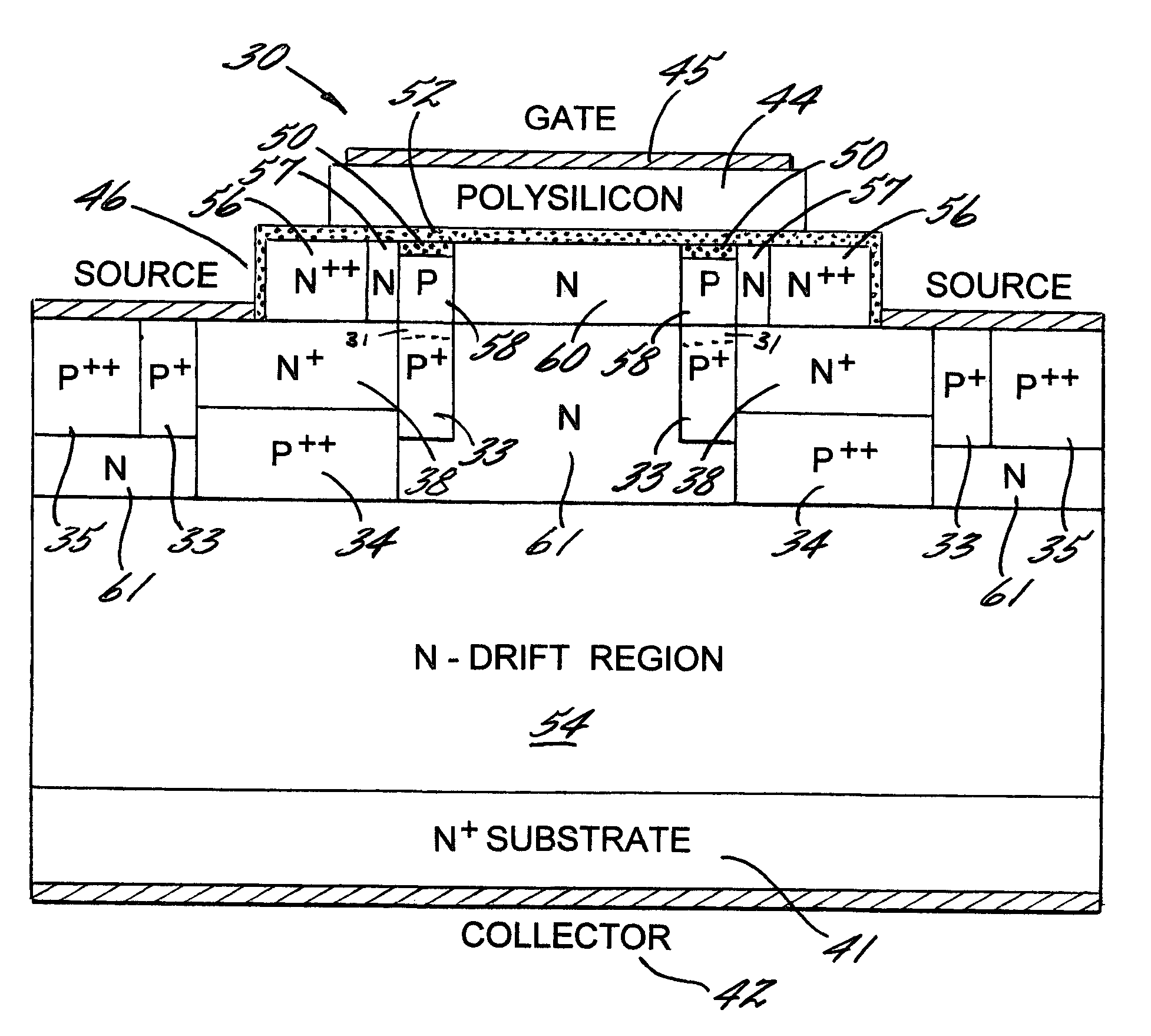
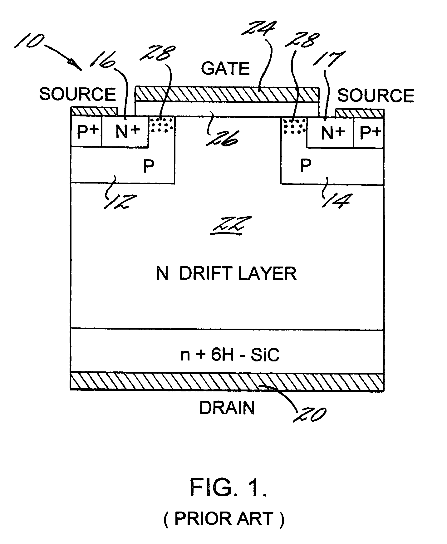
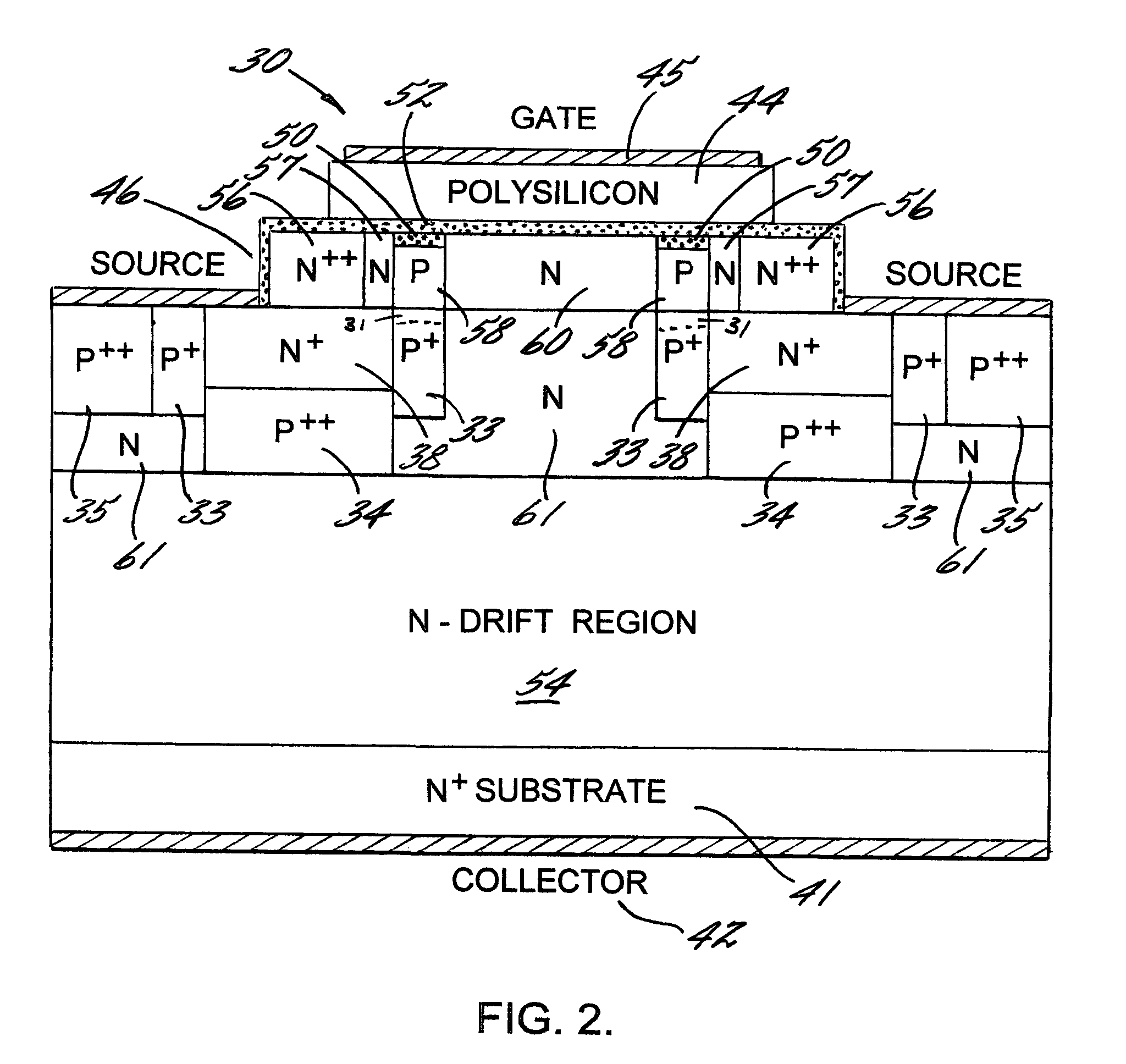
[0024]The invention is a device for controlling electrical conduction across a semiconductor body, particularly useful for metal-oxide-semiconductor field effect transistors (MOSFETs) (30), insulated gate bipolar transistors (IGBTs) (65), and other semiconductor devices used in power applications across a wide range of temperatures. The transistors disclosed herein incorporate a new P type regrown channel layer (46, 66) over the P type well (33, 83) that surrounds the transistor source region (38, 78).

[0025]This detailed description should not limit the invention to literal terms. For example, terms describing relative position of elements in this invention should be given their broadest meaning unless otherwise noted. For example, when a transistor element or layer is located “on” another layer, “beside” another element, or “adjacent” or “proximate” a certain part of the device at hand, that terminology suggests that intervening parts of the device may be present between the recite...


PUM


Abstract

The invention is a device for controlling conduction across a semiconductor body with a P type channel layer between active semiconductor regions of the device and the controlling gate contact. The device, often a MOSFET or an IGBT, includes at least one source, well, and drift region. The P type channel layer may be divided into sections, or divided regions, that have been doped to exhibit N type conductivity. By dividing the channel layer into regions of different conductivity, the channel layer allows better control over the threshold voltage that regulates current through the device. Accordingly, one of the divided regions in the channel layer is a threshold voltage regulating region. The threshold-voltage regulating region maintains its original P type conductivity and is available in the transistor for a gate voltage to invert a conductive zone therein. The conductive zone becomes the voltage regulated conductive channel within the device.

Description

BACKGROUND[0001]The invention relates to the field of semiconductor transistors utilizing a voltage applied to a gate contact to control current in a conductive channel. The device disclosed herein is particularly useful in the art of power transistors that operate in a wide range of temperatures. Transistors formed by the new method include a regrown P type epitaxial layer for the channel layer and thus exhibit better control at room temperature or even elevated temperatures.[0002]Numerous efforts have been underway to develop silicon carbide MOSFETs using conventional DMOS (double diffused metal-oxide-semiconductor) structures with an N type regrown channel that improves channel mobility. The presence of the N type regrown channel causes inherent fluctuations in device performance because the threshold voltage shifts with operating conditions. Research shows that the varying threshold voltage results, at least in part, from scattered carriers distributed through the device during ...

Claims


Application Information

Patent Timeline
Patent Type & Authority Patents(United States)
IPC IPC(8): H01L29/78
CPCH01L29/1095H01L29/41766H01L29/66068H01L29/66712H01L29/7396H01L29/7802H01L29/0653H01L29/086H01L29/1608H01L29/365
Inventor ZHANG, QINGCHUNHANEY, SARAHAGARWAL, ANANT
Owner WOLFSPEED INC
Why Eureka
Try Eureka