Stacked module and manufacturing method thereof

a technology of stacked modules and manufacturing methods, which is applied in the manufacture of printed circuits, printed circuit aspects, solid-state devices, etc., can solve the problems of increasing product cost and defective goods, unable to process at one time, and still required processes for disposing of soldering balls and flax on the surface electrodes. , to achieve the effect of reducing the defective goods rate, reducing manufacturing costs, and improving quality of products

Active Publication Date: 2010-10-05
MURATA MFG CO LTD
View PDF22 Cites 72 Cited by
  • Summary
  • Abstract
  • Description
  • Claims
  • Application Information

AI Technical Summary

Benefits of technology

[0010]To overcome the problems described above, preferred embodiments of the present invention provide a stacked module and a simplified manufacturing method thereof which reduces the rate of defective goods, and significantly lowers the manufacturing cost. In addition, the quality of the produce is improved, and multiple stacked modules can be simultaneously manufactured.
[0013]Preferably, the stacked module manufacturing method further includes a step of fabricating a board ceramic green body having a low-temperature sintering ceramic as a primary component and having a green wiring pattern on at least one of the surface and inner side thereof, a step of fabricating a shrinkage suppressing ceramic green body having a hard-to-sinter ceramic as a primary component which is not sintered with the low-temperature sintering ceramic, and having a green via conductor defining the bump electrode, a step of layering the shrinkage suppressing ceramic green body on at least one principal surface of the board ceramic green body, a step of baking both of the ceramic green bodies at a baking temperature for the low-temperature sintering ceramics, and while sintering the board ceramic green body, integrating the green wiring pattern and the green via conductor by simultaneous sintering, and a step of removing the shrinkage suppressing ceramic green body.
[0034]According to preferred embodiments of the present invention, a stacked module and a manufacturing method thereof are provided which simplify the manufacturing process thereof, reduce the rate of defective goods, and lower the cost significantly. In addition, the quality of the product is improved, and multiple stacked modules can be simultaneously produced.

Problems solved by technology

Therefore, the adhesion members, such as the spheres, cannot be processed at one time as is the case with a printed paste, but rather, the spheres must be disposed one at a time, or a specialized collet must be used for disposing the spheres.
Therefore, when connecting the boards to one another, the manufacturing processes for forming a connecting bump as described above increase substantially, and since a large amount of time and effort are required, the product cost and the rate of defective goods are increased.
However, the processes for painting flax on the surface electrode and for disposing the soldering ball are still required.
In addition, because of the complications involved in the process, a region in the vicinity of the soldering balls must be provided in which certain components cannot be mounted, which prevents the size of the product from being sufficiently reduced.

Method used


Image

  • Stacked module and manufacturing method thereof
  • Stacked module and manufacturing method thereof
  • Stacked module and manufacturing method thereof

Examples


first preferred embodiment

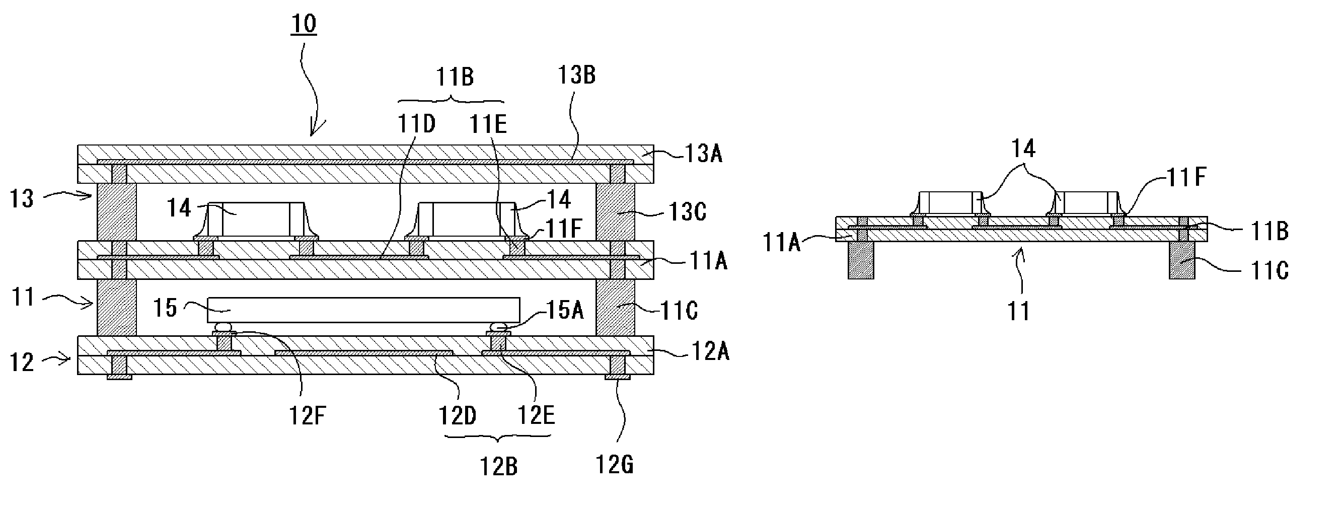
[0055]A stacked module 10 according to the present preferred embodiment, as shown in FIG. 1, includes a first wiring board 11, a second wiring board 12 disposed on the lower side of the first wiring board 11, a third wiring board 13 disposed on the upper side of the first wiring board 11, wherein the first, second, and third wiring boards 11, 12, and 13 are arranged so as to be layered with the first wiring board 11 disposed in the center in a vertical direction thereof, and, for example, can be configured to be mounted on a mounting board, such as a motherboard (not shown).

[0056]As shown in FIG. 1, the first wiring board 11 includes a board main unit 11A preferably made of a ceramic material, for example, a wiring pattern 11B provided on the board main unit 11A in a predetermined pattern, multiple bump electrodes 11C which are connected to the wiring pattern 11B and which extend vertically downward from the first principal surface (lower surface) of the board main unit 11A. The fir...

second preferred embodiment

[0090]With the stacked module according to the present preferred embodiment, portions which are similar or equivalent to the above-described preferred embodiment will be described using the same reference numerals. The stacked module 10 of the present preferred embodiment includes a first wiring board 11, a second wiring board 12 which is connected on the lower side of the wiring board 11, and a third wiring board 13 which is connected on the upper side of the first wiring board 11, and the board configuration is similar to that of the above-described preferred embodiment. Accordingly, the first, second, and third wiring boards 11, 12, and 13 are fabricated using the substantially same procedures used for above-described preferred embodiment.

[0091]In addition, with the present preferred embodiment, as shown in FIG. 5A, the chip-type passive components 14, which are mounted on the first wiring board in the above-described preferred embodiment, are mounted on the lower surface of the ...

third preferred embodiment

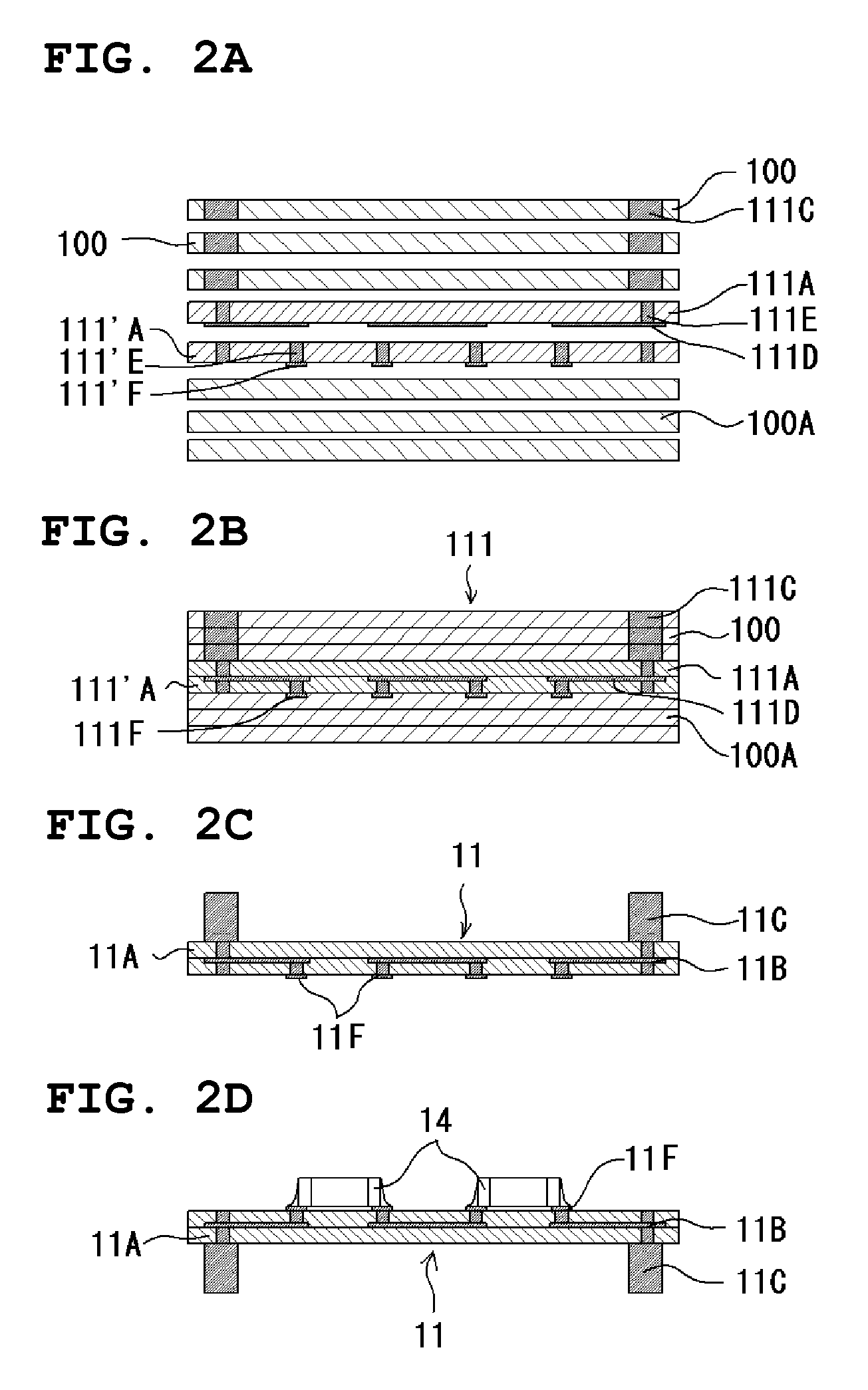
[0095]Each of the above-described preferred embodiments describes a case in which only one stacked module is fabricated. However, usually multiple stacked modules are fabricated simultaneously. Thus, with the present preferred embodiment, a method for fabricating multiple stacked modules simultaneously is described with reference to FIG. 6 and FIG. 7, wherein portions which are similar or equivalent to each of the above-described preferred embodiments will be described using the same reference numerals. With the present preferred embodiment, for example, multiple first wiring boards, second wiring boards, or third wiring boards can be fabricated from one board ceramic green sheet.

[0096]For example, in the case of fabricating multiple first wiring boards 11 simultaneously, the necessary number of board ceramic green sheets (not shown) for the first wiring board 11 is fabricated with the same procedures as for the first preferred embodiment. A green wiring pattern is independently pro...


PUM


Abstract

A manufacturing method of a stacked module includes a step of fabricating the first wiring board which includes a wiring pattern provided on at least one of a surface and an inner portion and a bump electrode which is integrated from the simultaneous sintering with the wiring pattern, and which extends in the vertical direction, a step of layering the first wiring board with the second wiring board having the wiring pattern provided on at least one of the surface and the inner portion thereof to be connected to the second wiring board via the bump electrode.

Description

BACKGROUND OF THE INVENTION[0001]1. Field of the Invention[0002]The present invention relates to a stacked module including multiple wiring boards that are layered in a vertical direction, a stacked module in which each layer of the wiring boards can be precisely connected, and a manufacturing method thereof.[0003]2. Description of the Related Art[0004]In general, technology of this type has been disclosed in Japanese Unexamined Patent Application Publication No. 7-263625 (Patent Document 1), Japanese Unexamined Patent Application Publication No. 8-236694 (Patent Document 2, Japanese Unexamined Patent Application Publication No. 11-8474 (Patent Document 3), and Japanese Unexamined Patent Application Publication No. 11-251515 (Patent Document 4).[0005]In Patent Document 1, a vertical layered IC chip article is disclosed which includes a discrete chip carrier made of a dielectric tape. This layered IC chip article includes a substrate including multiple fused dielectric tape layers an...

Claims


Application Information

Patent Timeline
Patent Type & Authority Patents(United States)
IPC IPC(8): H01L21/00
CPCH01L24/97H01L25/105H01L25/162H01L25/50H05K1/144H05K3/4007H01L25/0652H01L2924/07802H01L2225/107H01L2225/1058H01L2225/1023H01L2225/1088H01L2224/16225H01L2224/48091H01L2224/48227H01L2224/97H01L2924/01004H01L2924/01015H01L2924/01027H01L2924/01029H01L2924/01042H01L2924/01046H01L2924/01047H01L2924/01074H01L2924/01078H01L2924/01079H01L2924/09701H01L2924/14H01L2924/15331H01L2924/19041H01L2924/19042H01L2924/19105H01L2924/3025H05K1/0306H05K1/092H05K3/3436H05K3/4611H05K3/4629H05K2201/0367H05K2201/09481H05K2203/308H01L2924/01005H01L2924/01006H01L2924/01033H01L2924/00014H01L2224/81H01L2924/00H01L2924/351H01L2924/15787H01L2924/181H01L2924/1627H01L2924/00012
Inventor NISHIZAWA, YOSHIHIKO
Owner MURATA MFG CO LTD
Why Eureka
Try Eureka