Nonvolatile semiconductor memory and method for manufacturing the same

a non-volatile, memory technology, applied in semiconductor devices, instruments, electrical devices, etc., can solve the problems of limit of microminiaturization and increase in cost attributable to three-dimensional integration of memory cells

Active Publication Date: 2010-10-26
KIOXIA CORP
View PDF6 Cites 90 Cited by
  • Summary
  • Abstract
  • Description
  • Claims
  • Application Information

AI Technical Summary

Problems solved by technology

However, there are limits of the microminiaturization.
Moreover, in many semiconductor storage devices, memory cells are simply stacked one on top of the other, which unavoidably results in an increase in cost attributable to three-dimensional integration of memory cells.

Method used


Image

  • Nonvolatile semiconductor memory and method for manufacturing the same
  • Nonvolatile semiconductor memory and method for manufacturing the same
  • Nonvolatile semiconductor memory and method for manufacturing the same

Examples


first embodiment

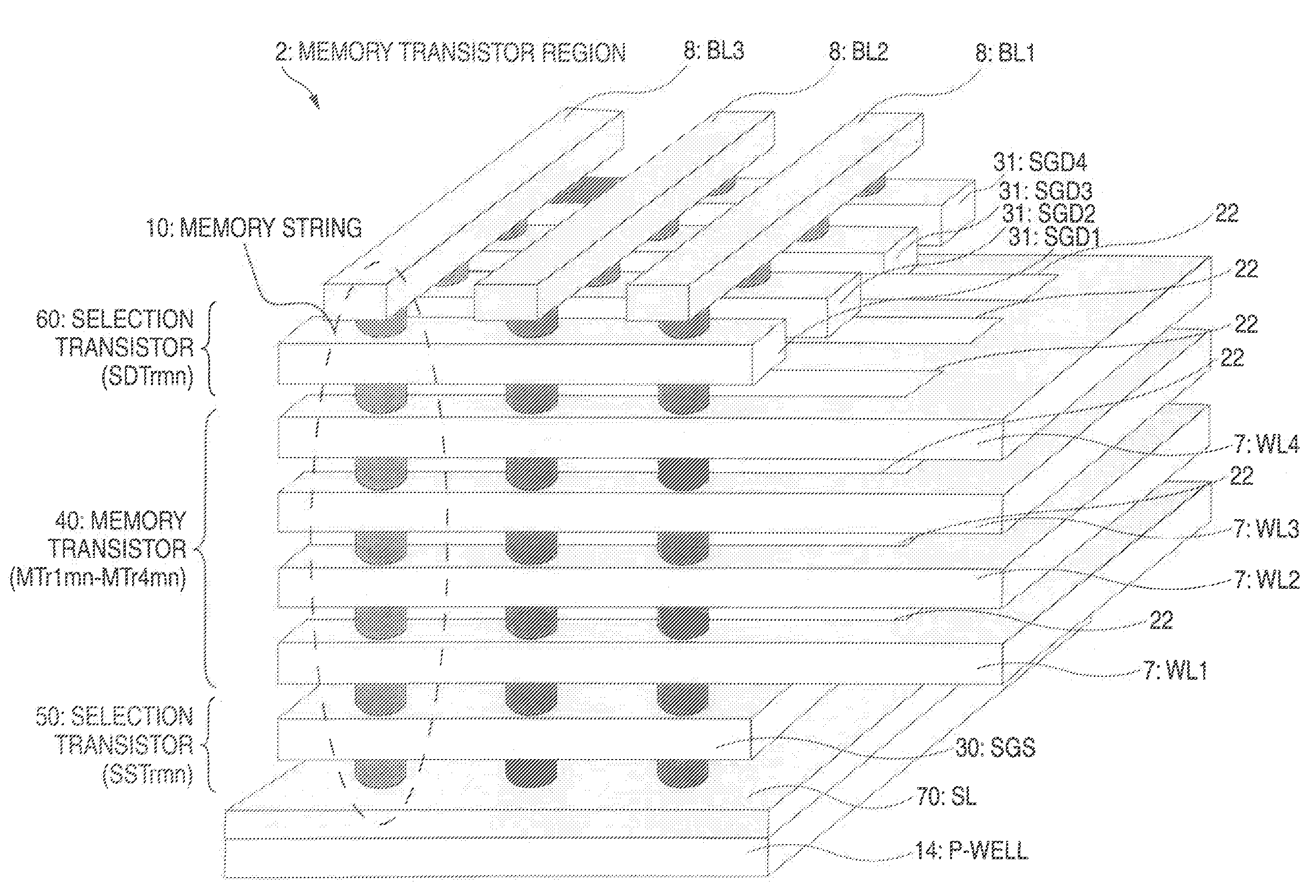
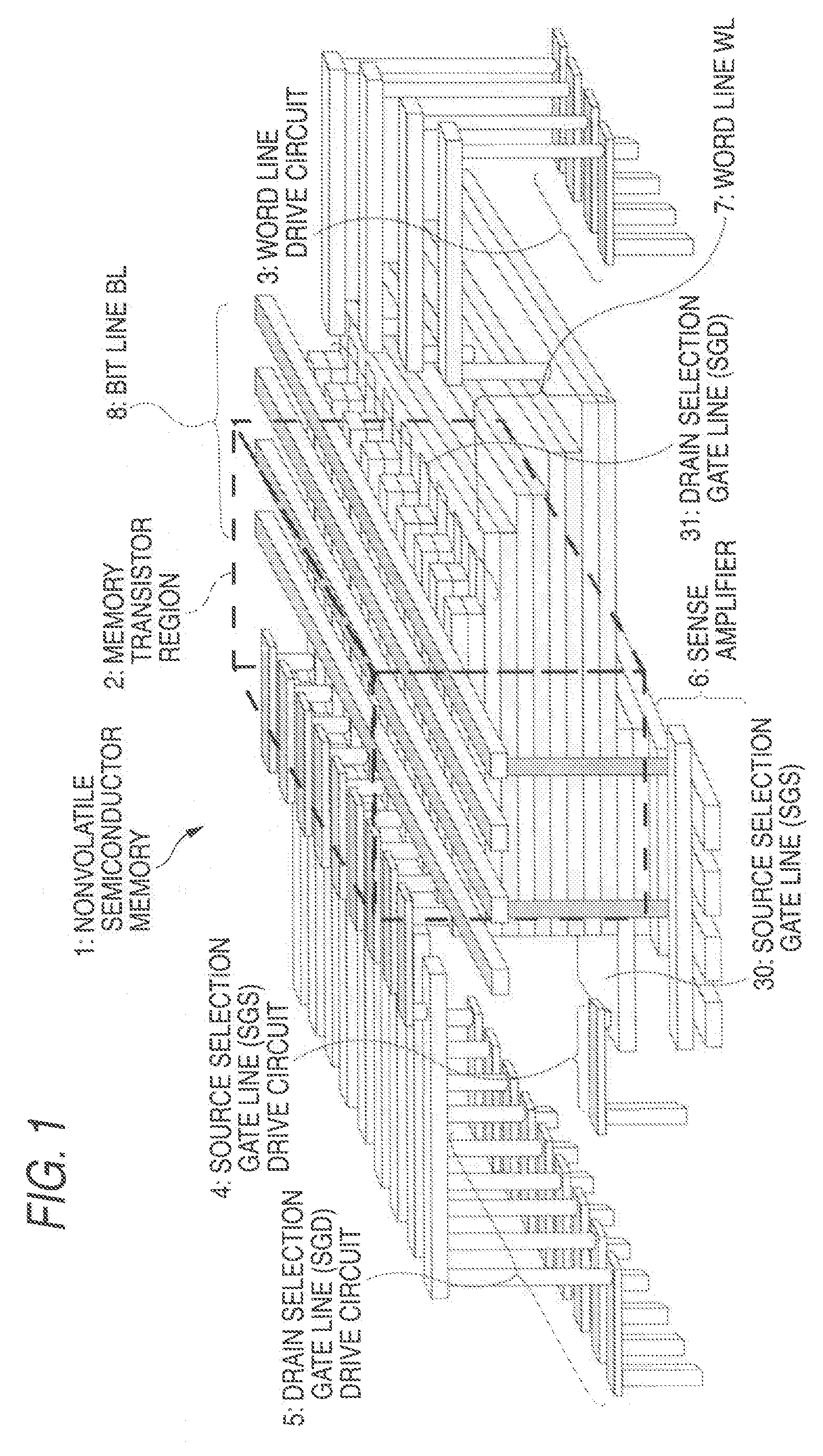
[0046]FIG. 1 is a drawing to show the schematic configuration of a nonvolatile semiconductor memory 1 according to a first embodiment. The nonvolatile semiconductor memory 1 according to the first embodiment has a memory transistor region 2, word line drive circuits 3, source selection gate line (SGS) drive circuits 4, drain selection gate line (SOD) drive circuits 5, sense amplifiers 6, word lines (WL) 7, bit lines (BL) 8, source selection gate lines (SGS) 30, drain selection gate lines (SGD) 31, etc. As shown in FIG. 1, in the nonvolatile semiconductor memory 1 according to the embodiment, memory transistors of the memory transistor regions 2 are formed on collectively stacked semiconductor layers. As shown in FIG. 1, each of the word lines (WL) 7 is a layer spread two-dimensionally and is formed of one conductive layer for each layer. In each layer, the word line has linear portions. The linear portions are connected at ends. In other words, the word line (WL) 7 has a shape of a ...

second embodiment

[0087]In the first embodiment described above, a slit is formed for each memory string column as shown in FIG. 2 and the sides of each slit are formed with metal silicide. In a second embodiment, an example will be discussed wherein a slit is provided every several memory string columns and the sides of each slit are formed with metal silicide instead of forming a slit for each memory string column.

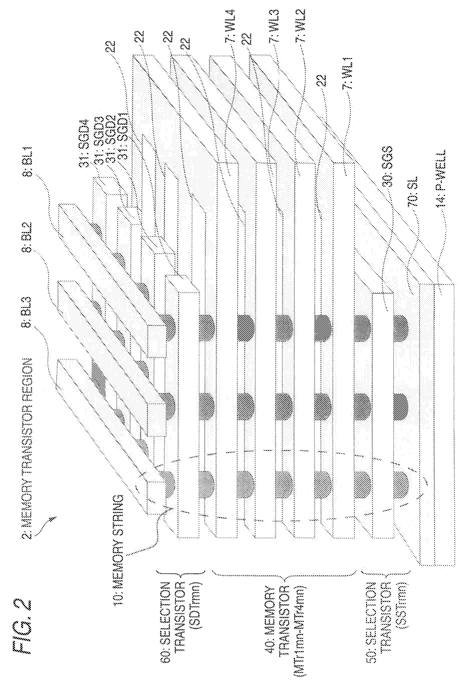
[0088]FIG. 20 is a drawing to show the schematic configuration of a part of a memory transistor region 2 of a nonvolatile semiconductor memory 1 according to the second embodiment. In the embodiment, the memory transistor region 2 has m×n memory strings 10 (where m and n are each a natural number) each made up of memory transistors (MTr1mn to MTr4mn) 40 and selection transistors SSTrmn 50 and SDTrmn 60. In FIG. 20, m=3 and n=4 by way of example, as with the first embodiment. Components similar to those of the nonvolatile semiconductor memory 1 according to the first embodiment will not be...


PUM


Abstract

According to an aspect of the present invention, there is provided a nonvolatile semiconductor memory including: a columnar semiconductor; a charge storage insulating film including: a first insulating film formed around the columnar semiconductor, a charge storage film formed around the first insulating film, and a second insulating film formed around the charge storage film; an electrode extending two-dimensionally to surround the charge storage insulating film, the electrode having a groove; and a metal silicide formed on a sidewall of the groove.

Description

CROSS-REFERENCE TO RELATED APPLICATIONS[0001]The entire disclosure of Japanese Patent Application No. 2007-002152 filed on Jan. 10, 2007 including specification, claims, drawings and abstract is incorporated herein by reference in its entirety.BACKGROUND OF THE INVENTION[0002]1. Field of the Invention[0003]An aspect of the present invention relates to an electrically rewritable semiconductor memory and in particular to a nonvolatile semiconductor memory.[0004]2. Description of the Related Art[0005]Demand for small-sized and large-capacity nonvolatile semiconductor memory grows sharply. Among the nonvolatile semiconductor memory, particularly, flash memory is used in various applications and a request is made for putting flash memory into a further larger capacity. Microminiaturization of the flash memory is acceleratively advancing, and thus a physical limit of the microminiaturization is being approached. With a structure where memory cells, circuit elements, etc., are placed on a ...

Claims


Application Information

Patent Timeline
Patent Type & Authority Patents(United States)
IPC IPC(8): H01L27/115H01L21/8247H01L29/792
CPCH01L27/11568H01L27/11578H01L27/11582H01L29/66833H01L29/792H01L29/7926G11C16/0483H01L27/0688H10B43/20H10B43/30H10B43/27
Inventor KIDOH, MASARUKATSUMATA, RYOTAKITO, MASARUFUKUZUMI, YOSHIAKIAOCHI, HIDEAKITANAKA, HIROYASUMATSUOKA, YASUYUKIOZAWA, YOSHIOSATO, MITSURU
Owner KIOXIA CORP
Why Eureka
Try Eureka