Fin-type field effect transistor structure with merged source/drain silicide and method of forming the structure

a field effect transistor and silicide technology, applied in the field of fin-type field-effect transistors, can solve the problems of series resistance limitation of drive current, and achieve the effect of reducing series resistance and increasing parasitic capacitan

Active Publication Date: 2010-12-14
GLOBALFOUNDRIES U S INC
View PDF25 Cites 107 Cited by
  • Summary
  • Abstract
  • Description
  • Claims
  • Application Information

AI Technical Summary

Benefits of technology

[0009]In view of the foregoing, disclosed herein are embodiments of a multiple fin fin-type field effect transistor (i.e., a multiple fin dual-gate or tri-gate field effect transistor) in which the multiple fins are partially or completely merged by a highly conductive material (e.g., a metal silicide). Merging the fins in this manner allow series resistance to be minimized with little, if any, increase in the parasitic capacitance between the gate electrode and source / drain regions. Merging the semiconductor fins in this manner also allows merged source / drain regions to be contacted by a single contact via as well as more flexible placement of that contact via.

Problems solved by technology

However, as the size of such FET structures is scaled, drive current becomes limited by series resistance.

Method used


Image

  • Fin-type field effect transistor structure with merged source/drain silicide and method of forming the structure
  • Fin-type field effect transistor structure with merged source/drain silicide and method of forming the structure
  • Fin-type field effect transistor structure with merged source/drain silicide and method of forming the structure

Examples


Embodiment Construction

[0041]The embodiments of the invention and the various features and advantageous details thereof are explained more fully with reference to the non-limiting embodiments that are illustrated in the accompanying drawings and detailed in the following description. It should be noted that the features illustrated in the drawings are not necessarily drawn to scale. Descriptions of well-known components and processing techniques are omitted so as to not unnecessarily obscure the embodiments of the invention. The examples used herein are intended merely to facilitate an understanding of ways in which the embodiments of the invention may be practiced and to further enable those of skill in the art to practice the embodiments of the invention. Accordingly, the examples should not be construed as limiting the scope of the embodiments of the invention.

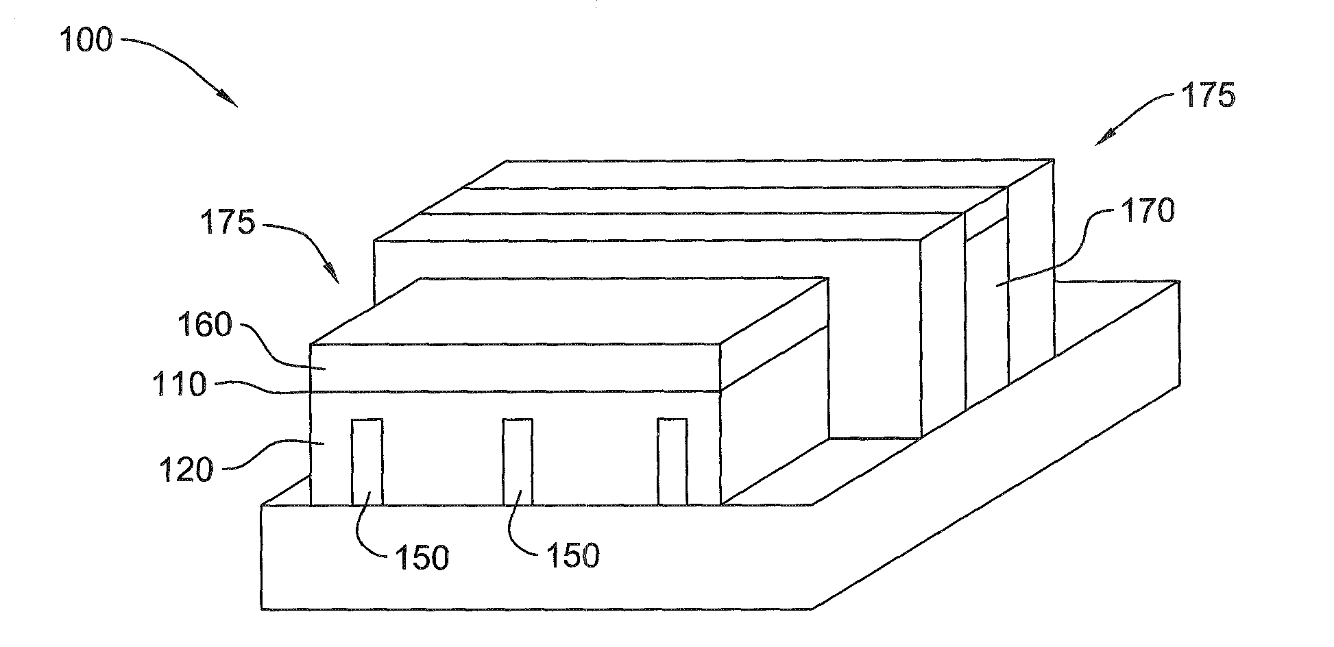
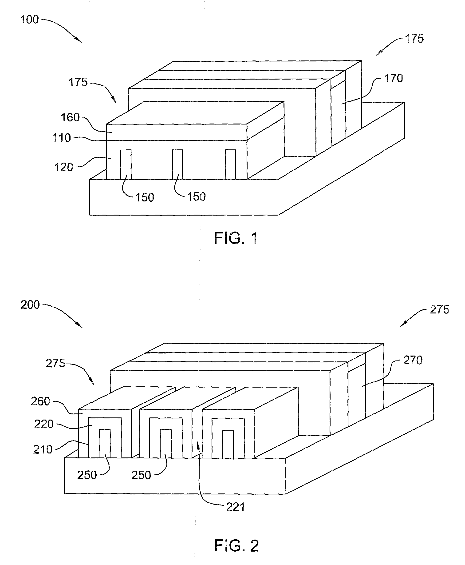
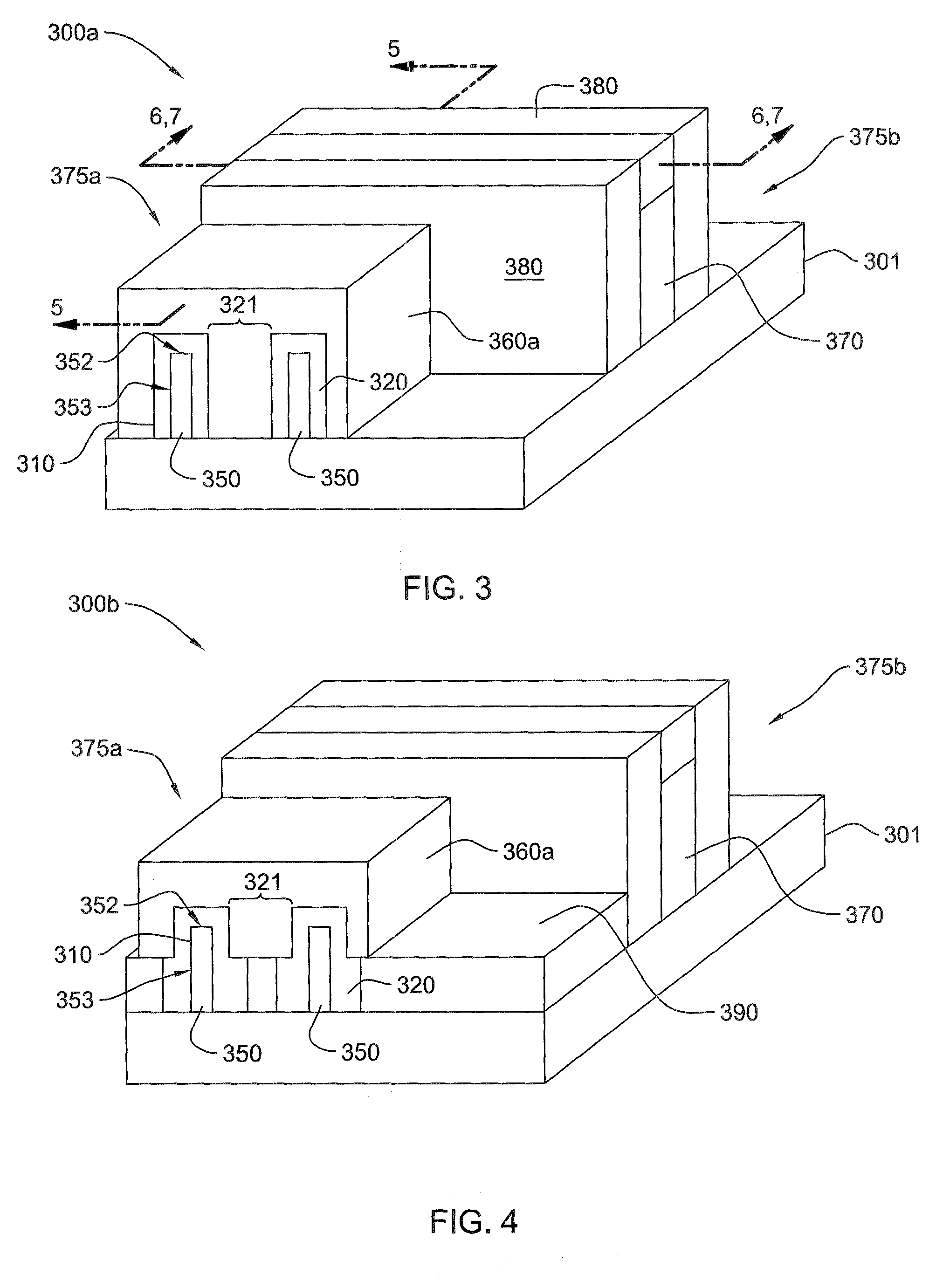
[0042]As mentioned above, the effective channel width of both dual-gate and tri-gate fin-type field effect transistors can be increased by incor...


PUM


Abstract

Disclosed herein are embodiments of a design structure of a multiple fin fin-type field effect transistor (i.e., a multiple fin dual-gate or tri-gate field effect transistor) in which the multiple fins are partially or completely merged by a highly conductive material (e.g., a metal silicide). Merging the fins in this manner allow series resistance to be minimized with little, if any, increase in the parasitic capacitance between the gate and source / drain regions. Merging the semiconductor fins in this manner also allows each of the source / drain regions to be contacted by a single contact via as well as more flexible placement of that contact via.

Description

CROSS-REFERENCE TO RELATED APPLICATIONS[0001]This application is related to application Ser. No. 11 / 778,217 filed Jul. 16, 2007, the complete disclosure of which, in its entirety, is herein incorporated by reference.BACKGROUND[0002]1. Field of the Invention[0003]The embodiments of the invention generally relate to fin-type field effect transistors and, more particularly, to a fin-type field effect transistor having multiple fins which are merged by a conductor (e.g., a metal silicide).[0004]2. Description of the Related Art[0005]As transistor design is improved and evolves, the number of different types of transistors continues to increase. Multi-gated non-planar metal oxide semiconductor field effect transistors, including dual-gate fin-type FETs and tri-gate fin-type FETs, were developed to provide scaled devices with faster drive currents and reduced short channel effects over planar FETs.[0006]A dual-gate fin-type FET is a FET in which the channel region is formed in the center ...

Claims


Application Information

Patent Timeline
Patent Type & Authority Patents(United States)
IPC IPC(8): H01L29/78
CPCH01L29/66795H01L29/785
Inventor ANDERSON, BRENT A.BRYANT, ANDRESELLIS-MONAGHAN, JOHN J.NOWAK, EDWARD J.
Owner GLOBALFOUNDRIES U S INC
Why Eureka
Try Eureka