Mos transistor for reducing short-channel effects and its production

a technology of short-channel effects and transistors, which is applied in the direction of semiconductor devices, basic electric elements, electrical appliances, etc., can solve the problems of increasing leakage current even a breakdown of the gate, increasing the thickness of the existing gate insulation layer, and reducing the short-channel effect, so as to reduce the short-channel

Active Publication Date: 2011-03-10
SHANGHAI INTEGRATED CIRCUIT RES & DEV CENT
View PDF11 Cites 102 Cited by
  • Summary
  • Abstract
  • Description
  • Claims
  • Application Information

AI Technical Summary

Benefits of technology

[0006]An objective of the invention is to provide a metal-oxide semiconductor (MOS) transistor for reducing short-channel effects and its fabrication method. It makes a gate stack in a groove lower than the top surface of source and drain areas to get a relative elevated source and drain structure. And thereby the short-channel effects can be effectively reduced with less technology difficulty and cost. Furthermore, the height of the gate stack can be reduced to provide a larger process window for the subsequent process of pre-metal dielectric deposition.
[0007]To achieve the above objective, the invention provides a MOS transistor for reducing short-channel effects. The MOS transistor is fabricated on a silicon substrate after an isolation module is finished, and the MOS transistor includes a gate stack and source and drain areas. Wherein the silicon substrate has a groove and the gate stack is formed in the groove.
[0008]In the MOS transistor for reducing short-channel effects, the bottom of the groove is lower than the top surface of the source and drain areas.

Problems solved by technology

However, short-channel effects will arise when the channel length shortened to a certain degree, leading to the worsening of device performance, even malfunctioning.
However, the thinness of the existing gate insulation layer has approached a limit; that is, when further decreasing the thickness, an increasing leakage current even a breakdown will easily arise in the gate.
Therefore, further decreasing the thickness of a gate insulation layer is not an effective method for reducing the short-channel effects.
In addition, by producing a source and drain structure with shallow junctions to reduce the short-channel effects is also difficult to achieved.
However, the epitaxial technique is difficult to control and has the problem of high complexity, high cost, high defect density, etc.

Method used


Image

  • Mos transistor for reducing short-channel effects and its production
  • Mos transistor for reducing short-channel effects and its production
  • Mos transistor for reducing short-channel effects and its production

Examples


Embodiment Construction

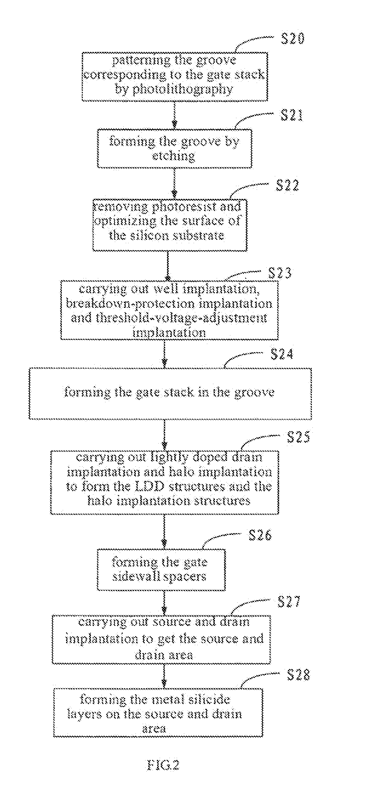
[0024]The metal-oxide semiconductor (MOS) transistor for reducing short-channel effects and its fabrication of the invention will be described in detail thereinafter.

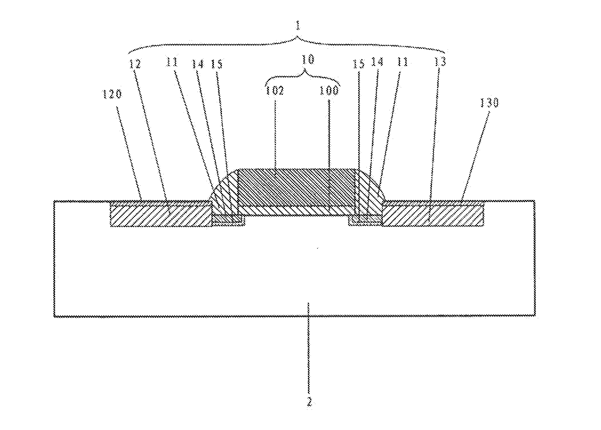
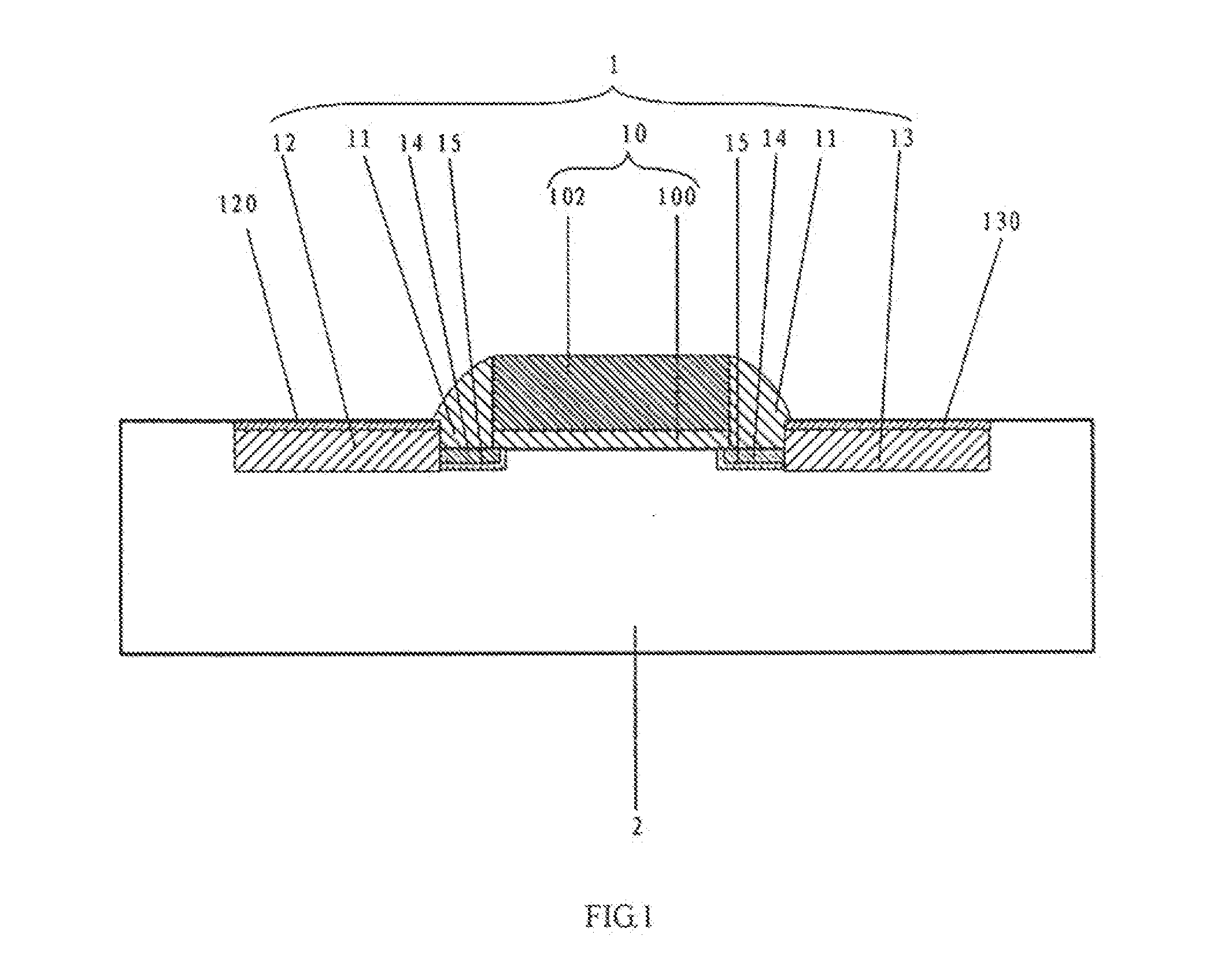
[0025]As shown in FIG. 1, the MOS transistor 1 for reducing short-channel effects is produced on a silicon substrate 2 after an isolation module is finished. The MOS transistor 1 includes a gate stack 10, gate sidewall spacer 11, source 12 and drain 13 areas, lightly doped drain (LDD) structures 14, and halo implantation structures 15.

[0026]The gate stack 10 includes a gate insulation layer 100 and a gate electrode 102. The silicon substrate 2 has a groove 20 (shown in FIG. 4) for receiving the gate stack 10, wherein the bottom of the groove 20 is lower than the top surface of the source 12 and drain 13 areas. Thereby the gate stack 10 formed in the groove 20 will have a bottom surface lower than the top surface of the source 12 and drain 13 areas to get a relative elevated source and drain structure. In addition, the a...


PUM


Abstract

The invention is related to a MOS transistor and its fabrication method to reduce short-channel effects. Existing process has the problem of high complexity and high cost to reduce short-channel effects by using epitaxial technique to produce an elevated source and drain structure. In the invention, the MOS transistor, fabricated on a silicon substrate after an isolation module is finished, includes a gate stack, a gate sidewall spacer, and source and drain areas. The silicon substrate has a groove and the gate stack is formed in the groove. And the process for the MOS transistor includes the following steps: forming the groove; carrying out well implantation, anti-punchthrough implantation and threshold-voltage adjustment implantation; forming the gate stack in the groove which comprising patterning the gate electrode; carrying lightly doped drain implantation and halo implantation; forming the gate sidewall spacer; carrying source and drain implantation to get the source and drain areas; forming a metal silicide layer on the source and drain areas.

Description

BACKGROUND OF THE INVENTION[0001]1. Field of the Invention[0002]The invention relates to semiconductor product and, more particularly, to a metal-oxide semiconductor (MOS) transistor for reducing short-channel effects.[0003]2. Description of Related Art[0004]Semiconductor devices can work faster by scaling down their dimensions. Therefore the channel length of a metal-oxide semiconductor (MOS) transistor is being scaled down. However, short-channel effects will arise when the channel length shortened to a certain degree, leading to the worsening of device performance, even malfunctioning. The short-channel effects can be reduced by decreasing the thickness of a gate insulation layer or producing a source and drain structure with shallow junctions. However, the thinness of the existing gate insulation layer has approached a limit; that is, when further decreasing the thickness, an increasing leakage current even a breakdown will easily arise in the gate. Therefore, further decreasing...

Claims


Application Information

Patent Timeline
Patent Type & Authority Applications(United States)
IPC IPC(8): H01L21/336
CPCH01L29/1083H01L29/665H01L29/7834H01L29/7833H01L29/66621
Inventor KANG, XIAOXU
Owner SHANGHAI INTEGRATED CIRCUIT RES & DEV CENT
Why Eureka
Try Eureka