

Method for forming an electronic structure using etch
a technology of electronic structure and etching, which is applied in the direction of semiconductor devices, electrical devices, nanotechnology, etc., can solve the problems of increasing fabrication costs proportional to the increase in the amount of etching, affecting the size reduction of mos transistors, and additional physical process limitations
- Summary
- Abstract
- Description
- Claims
- Application Information
AI Technical Summary
Problems solved by technology
Method used
Image

Examples
Embodiment Construction
For a thorough understanding of the subject invention, reference is made to the following Detailed Description, which includes the appended Claims, in connection with the above-described Drawings.
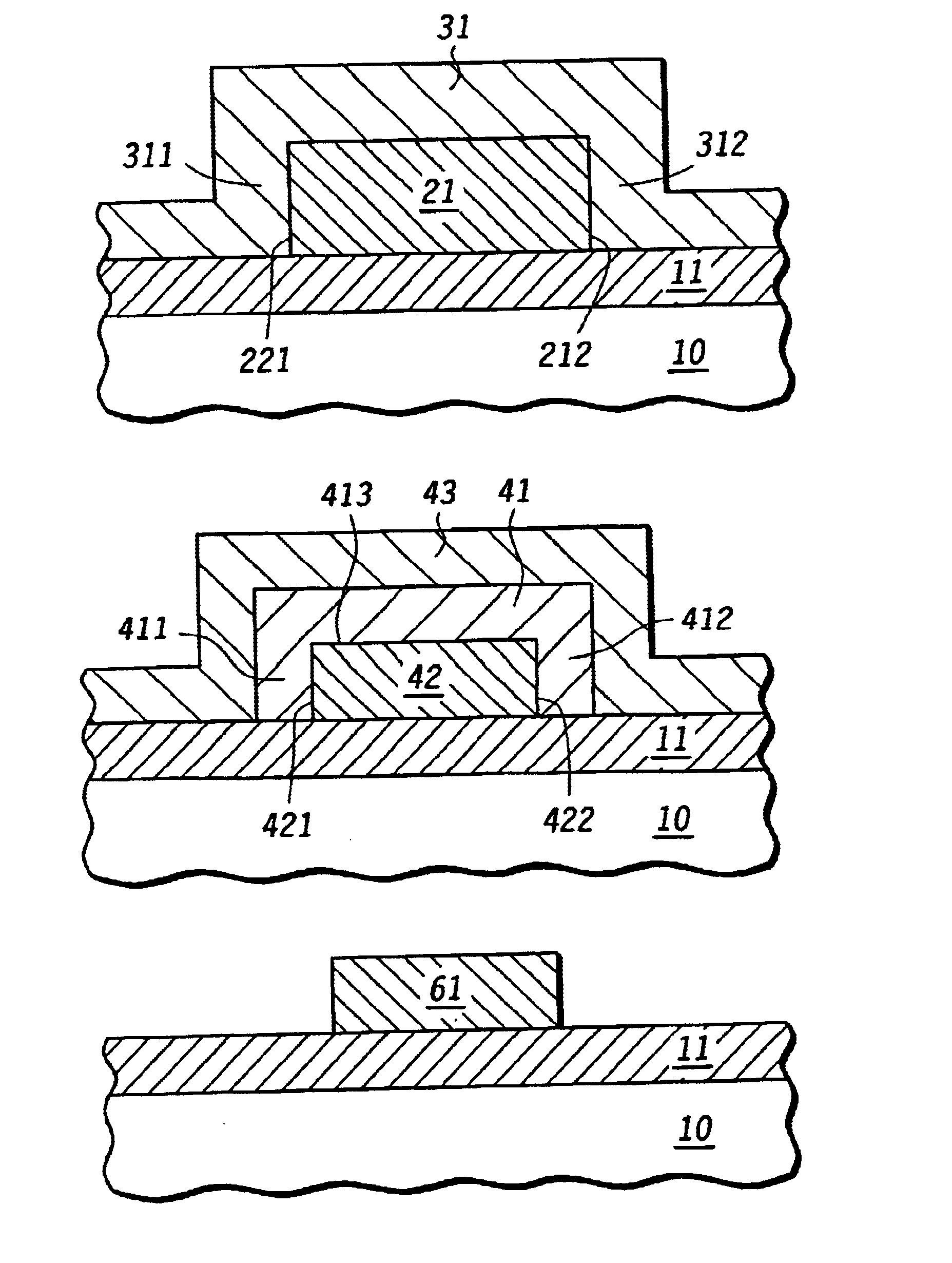
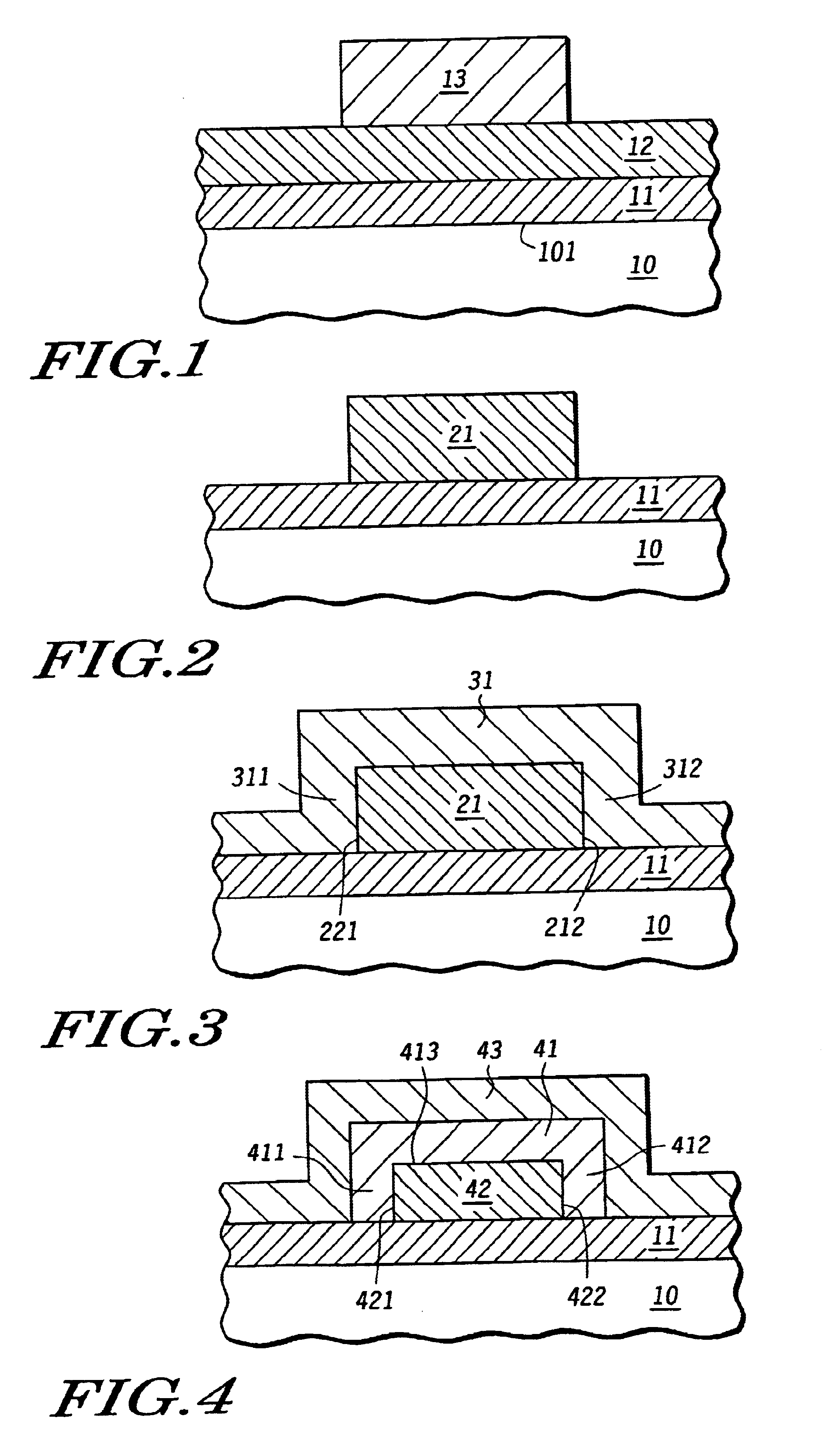
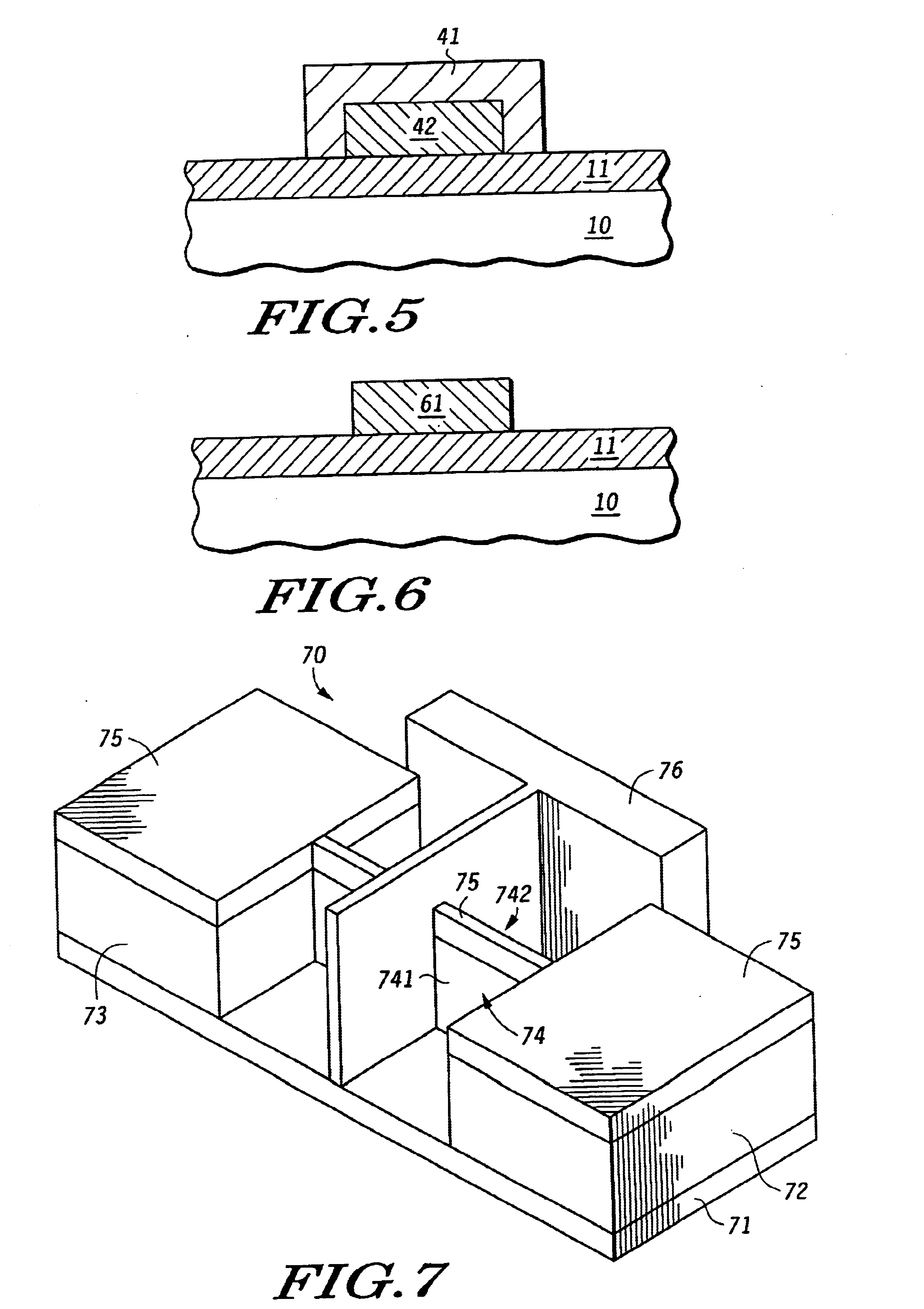
In a manner that will be made eminently clear below, the subject invention inheres, in one form, in a technique for directly achieving the ultimate length of a MOS transistor gate structure other than by a photolithographic step. The technique is particularly felicitous in fabrication processes where photolithography is unavailing, or contraindicated, as the process step for the formation of a reduced gate length. A polysilicon gate conductor layer is first formed on a metal oxide (MeOx) gate dielectric layer. The polysilicon layer is then photolithographically patterned to a first length. A metal layer is formed conformally over the patterned polysilicon. The metal is reacted with the polysilicon at a controlled temperature to form metal suicide sidewalls contiguous to the sidewalls of the...
PUM
 Abstract
Description
Claims
Application Information