

Contact plug structure, semiconductor device, and method for forming contact plug
- Summary
- Abstract
- Description
- Claims
- Application Information
AI Technical Summary
Benefits of technology
Problems solved by technology
Method used
Image

Examples
first embodiment
[0076]A metal silicide layer for forming a manganese oxide layer of the first embodiment of the present invention is formed at an active region of a transistor element that exerts functions of a source, drain, and / or gate composed of semiconductor silicon that are formed at surface parts of a substrate composed of silicon, glass, etc. The metal silicide layer is formed as an electrode, etc., at the active region of the transistor element composed of semiconductor silicon. The metal silicide is a chemical compound of a metallic element and silicon (Si). Examples of the metallic element are; magnesium (element symbol: Mg), platinum, (element symbol: Pt), hafnium (element symbol: Hf), molybdenum (element symbol: Mo), tantalum (Ta), vanadium (element symbol: V), niobium (element symbol: Nb) and chrome (element symbol: Cr). From the viewpoint of electrical characteristics, a metal silicide that includes any of cobalt (Co), titanium (Ti), nickel (Ni) and tungsten (W) is especially used in...
example 1
[0110]The contents of this invention will be explained by detailing an example where a contact plug which is made of copper (Cu) and has a nickel (Ni) silicide layer as the metal silicide layer is formed.
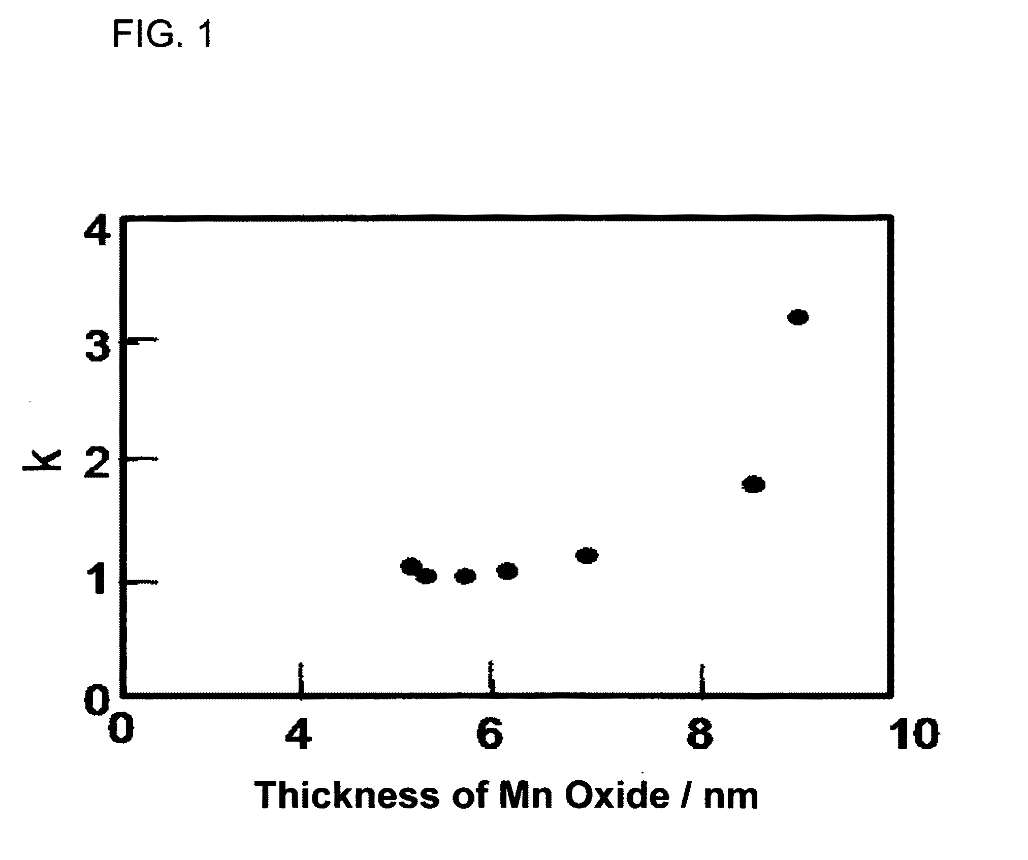
[0111]FIG. 2, FIG. 3, and FIG. 4 are figures that show the steps for forming the contact plug formed of copper (Cu) of this example. FIG. 5 is a cross-sectional transmission electron microscope (TEM) image of a laminated structure formed of a metal silicide (nickel (Ni) silicide) layer / a manganese oxide layer / copper (Cu). Moreover, FIG. 6 is an analysis figure that shows the binding state of manganese (Mn) that constitutes the manganese oxide layer.
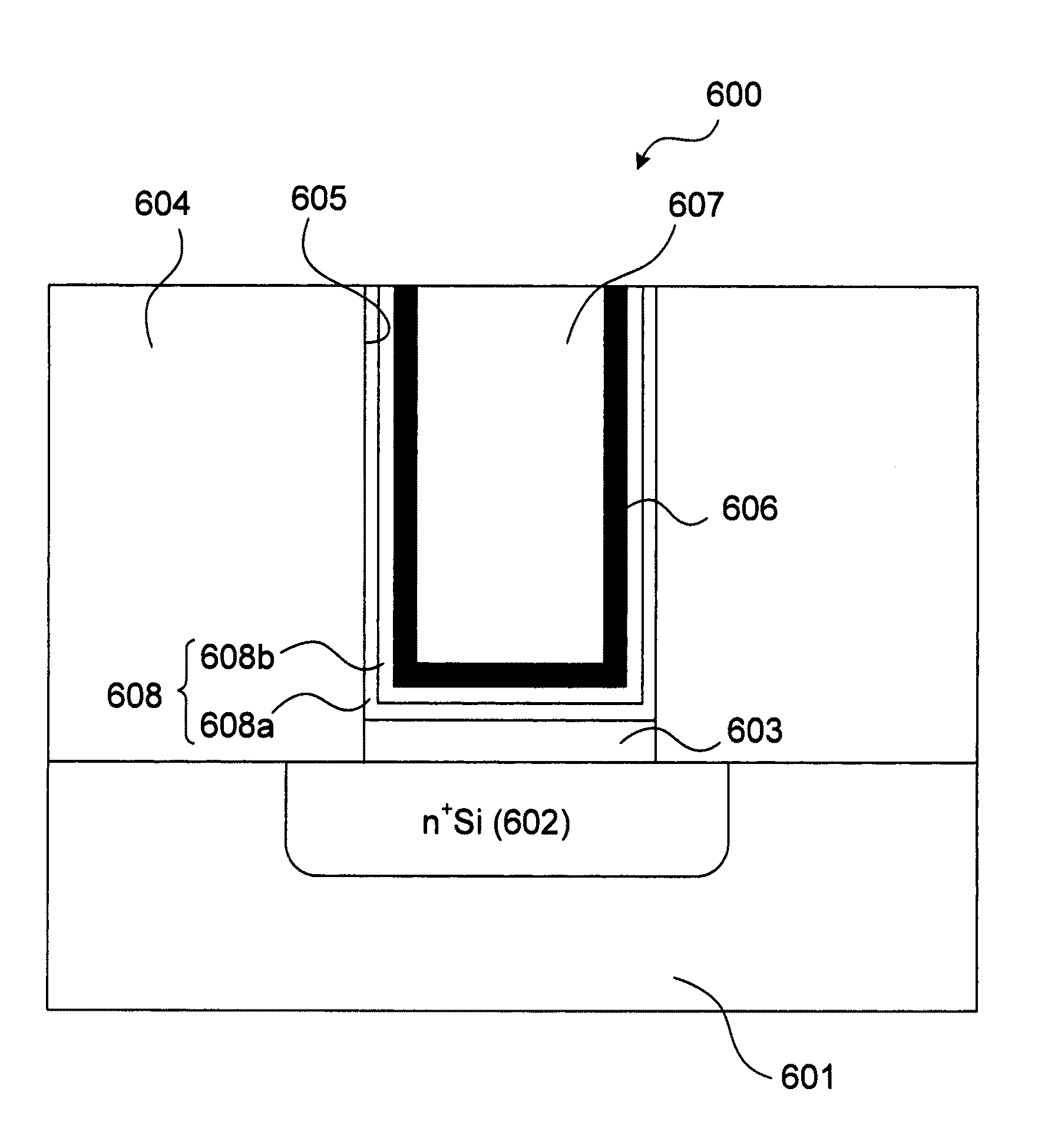
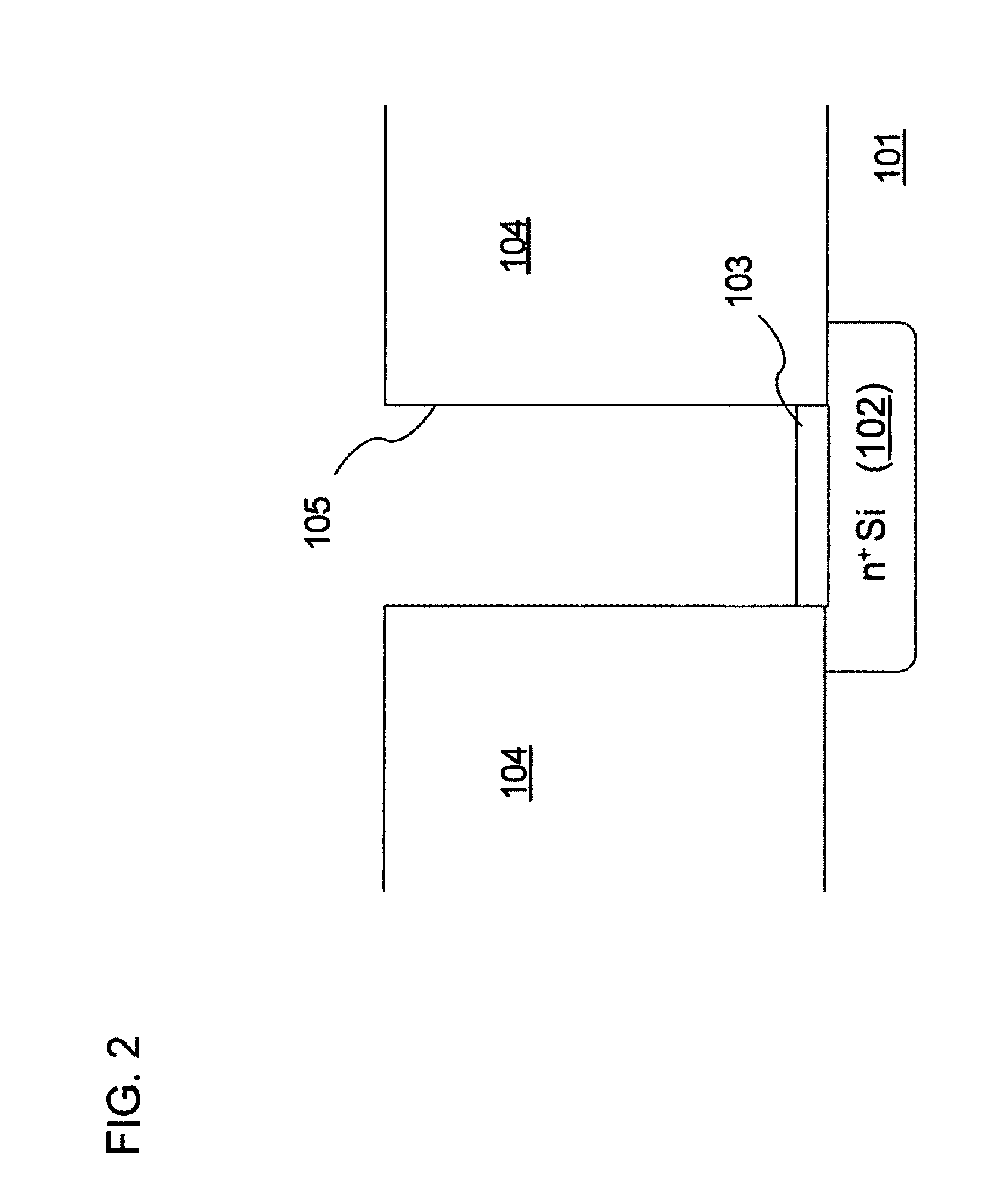
[0112]The steps for forming the contact plug formed of copper (Cu) will be explained using FIG. 2-FIG. 4. First, a nickel (Ni) layer is formed using a physical vapor deposition method in order to form a metal silicide layer 103 on the complete surface of a silicon substrate 101 (refer to FIG. 2) having an active region 102 of an n type co...
example 2
[0121]Next, FIG. 7 and FIG. 8 will be used to explain a case where a contact plug is manufactured after forming a manganese oxide layer and a buried copper by heating a copper-manganese alloy layer.
[0122]FIG. 7 is a pattern diagram that schematically shows steps for forming a manganese oxide layer and a buried copper by heating a copper-manganese alloy layer.
[0123]In FIG. 7(a), a silicon layer 202 is a substrate for forming a copper-manganese alloy. A thin cobalt layer is formed on the silicon layer 202 with thickness of 10 nm by a high frequency sputtering method. Then, heat treatment process is performed for one hour at 400° C. in vacuum, thereby changing the thin cobalt layer into the metal silicide layer 203 formed of cobalt. A plasma oxidation process is applied to this sample. The conditions for the plasma oxidization are; high-frequency output 100 W, oxygen pressure 40 Pa, at room temperature, and for 10 minutes. Using this process, the surface of the metal silicide layer 203...
PUM
 Abstract
Description
Claims
Application Information