Semiconductor device

a technology of semiconductor devices and semiconductors, applied in semiconductor devices, electrical devices, instruments, etc., can solve the problems of lowering the reliability of semiconductor devices in some cases, and lowering the reliability of semiconductor devices

Inactive Publication Date: 2014-01-02
SEMICON ENERGY LAB CO LTD
View PDF5 Cites 38 Cited by
  • Summary
  • Abstract
  • Description
  • Claims
  • Application Information

AI Technical Summary

Benefits of technology

[0008]In a semiconductor device using an oxide semiconductor, elements released from an insulating film or the like provided over an oxide semiconductor film including a channel formation region are diffused into the oxide semiconductor film as impurities, so that electrical characteristics (typically, a threshold voltage) of the semiconductor device are changed, which lowers the reliability of the semiconductor device in some cases.
[0009]For example, in the case where water and / or hydrogen, or nitrogen and / or ammonia is contained in the insulating film provided over the oxide semiconductor film, diffusion of any of water, hydrogen, nitrogen, and ammonia causes a change in electrical characteristics of the semiconductor device, which lowers the reliability of the semiconductor device.
[0011]Thus, an object of one embodiment of the present invention is to provide a semiconductor device including an oxide semiconductor in which a change in electrical characteristics is suppressed or whose reliability is improved.
[0019]In the semiconductor device, in the case where an organic resin film is provided in contact with the second insulating film and serves as an interlayer insulating film or a planarization insulating film, the second insulating film can suppress diffusion of water contained in the organic resin film and water in the air through the organic resin film into the oxide semiconductor film. As an example of the organic resin film, an acrylic film or the like can be given.
[0020]In the semiconductor device of one embodiment of the present invention, an insulating film which can fill oxygen vacancies included in an oxide semiconductor film is provided between the oxide semiconductor film and an insulating film which protects the oxide semiconductor film from elements released from the insulating film which suppresses entry of water. Specifically, an insulating film which is in contact with an oxide semiconductor film and through which oxygen penetrates and an insulating film which is in contact with the insulating film through which oxygen penetrates and which contains oxygen at a higher proportion than a stoichiometric composition are provided.
[0025]In the above semiconductor device, in the case where an organic resin film is provided in contact with the fourth insulating film to serve as an interlayer insulating film or a planarization insulating film, the fourth insulating film can suppress diffusion of water contained in the organic resin film and water in the air into the oxide semiconductor film through the organic resin film. For example, as the organic resin film, an acrylic film or the like can be given.

Problems solved by technology

In a semiconductor device using an oxide semiconductor, elements released from an insulating film or the like provided over an oxide semiconductor film including a channel formation region are diffused into the oxide semiconductor film as impurities, so that electrical characteristics (typically, a threshold voltage) of the semiconductor device are changed, which lowers the reliability of the semiconductor device in some cases.
For example, in the case where water and / or hydrogen, or nitrogen and / or ammonia is contained in the insulating film provided over the oxide semiconductor film, diffusion of any of water, hydrogen, nitrogen, and ammonia causes a change in electrical characteristics of the semiconductor device, which lowers the reliability of the semiconductor device.

Method used


Image

  • Semiconductor device
  • Semiconductor device
  • Semiconductor device

Examples


embodiment 1

[0054]In this embodiment, a semiconductor device of one embodiment of the present invention and a method for manufacturing the semiconductor device are described with reference to drawings. In this embodiment, a transistor including an oxide semiconductor film is described as an example of the semiconductor device.

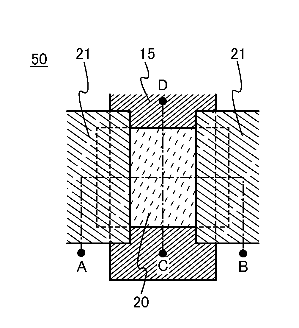
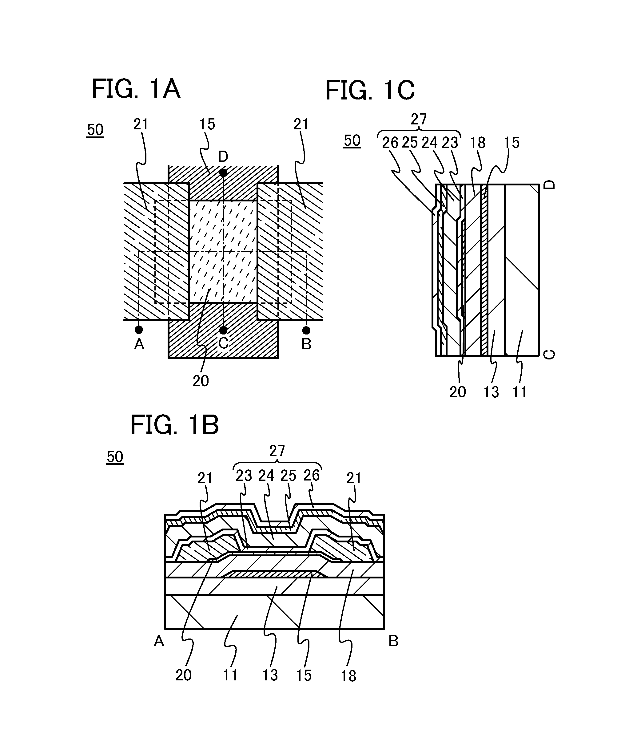
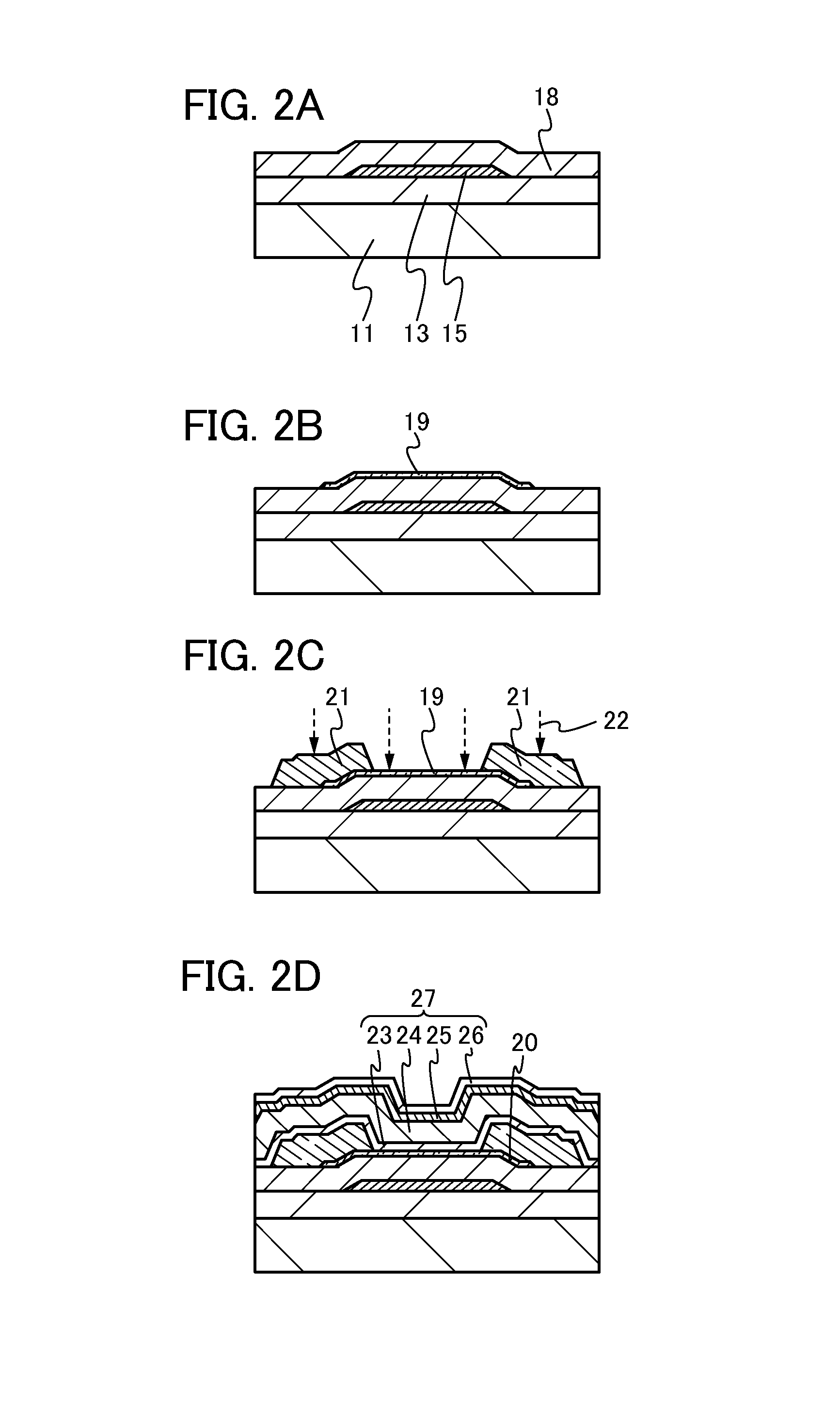
[0055]FIGS. 1A to 1C are a top view and cross-sectional views of a transistor 50. FIG. 1A is a top view of the transistor 50, FIG. 1B is a cross-sectional view taken along dashed-dotted line A-B in FIG. 1A, and FIG. 1C is a cross-sectional view taken along dashed-dotted line C-D in FIG. 1A. Note that in FIG. 1A, a substrate 11, a base insulating film 13, some components of the transistor 50 (e.g., a gate insulating film 18), insulating films 23 to 26, and the like are omitted for simplicity.

[0056]The transistor 50 is a bottom-gate transistor in which a gate electrode 15 is provided over the substrate 11. In the transistor 50, the gate insulating film 18 is provided over th...

embodiment 2

[0204]In this embodiment, a transistor having a structure different from that of Embodiment 1 is described with reference to FIG. 3. A transistor 70 of this embodiment includes a plurality of gate electrodes facing each other with an oxide semiconductor film provided therebetween.

[0205]The transistor 70 includes the gate electrode 15 provided over the substrate 11. Further, in the transistor 70, the gate insulating film 18 is provided over the substrate 11 and the gate electrode 15, the oxide semiconductor film 20 is provided to overlap with the gate electrode 15 with the gate insulating film 18 provided therebetween, and the pair of electrodes 21 is provided in contact with the oxide semiconductor film 20. In the transistor 70, at least the insulating films 25 and 26 are provided over the gate insulating film 18, the oxide semiconductor film 20, and the pair of electrodes 21. A gate electrode 61 is provided over the insulating film 26 to overlap with the oxide semiconductor film 20...

embodiment 3

[0209]A semiconductor device (also referred to as a display device) having a display function can be manufactured using the transistor of one embodiment of the present invention. Moreover, some or all of the driver circuits of the semiconductor device can be formed over a substrate where the pixel portion is formed, whereby a system-on-panel can be obtained.

[0210]In FIG. 4A, a sealant 905 is provided so as to surround a pixel portion 902 provided over a substrate 901, and the pixel portion 902 is sealed with a substrate 906. In FIG. 4A, a signal line driver circuit 903 and a scan line driver circuit 904 each are formed using a single crystal semiconductor film or a polycrystalline semiconductor film over an IC chip or a substrate prepared separately, and mounted in a region different from the region surrounded by the sealant 905 over the substrate 901. Further, various signals and potentials which are provided to the pixel portion 902 through the signal line driver circuit 903 and t...


PUM


Abstract

To provide a semiconductor device including an oxide semiconductor in which a change in electrical characteristics is suppressed or whose reliability is improved. In a semiconductor device including an oxide semiconductor film in which a channel formation region is formed, an insulating film which suppresses entry of water and contains at least nitrogen and an insulating film which suppresses entry of nitrogen released form the insulating film are provided over the oxide semiconductor film. As water entering the oxide semiconductor film, water contained in the air, water in a film provided over the insulating film which suppresses entry of water, or the like can be given. Further, as the insulating film which suppresses entry of water, a nitride insulating film can be used, and the amount of hydrogen molecules released by heating from the nitride insulating film is smaller than 5.0×10²¹ molecules / cm3.

Description

TECHNICAL FIELD[0001]The invention disclosed in this specification and the like relates to semiconductor devices.[0002]Note that a semiconductor device in this specification and the like refers to any device that can function by utilizing semiconductor characteristics, and for example, electro-optical devices, image display devices, semiconductor circuits, and electronic devices are all semiconductor devices.BACKGROUND ART[0003]For an image display device typified by a liquid crystal display device and a light-emitting display device, a transistor using a semiconductor thin film formed over a substrate having an insulating surface is utilized. Further, such a transistor is applied to a wide range of electronic devices such as an integrated circuit (IC). For the semiconductor thin film which can be applied to the transistor, not only a widely known silicon-based semiconductor but also a metal oxide showing semiconductor characteristics (hereinafter referred to as an oxide semiconduct...

Claims


Application Information

Patent Timeline
Patent Type & Authority Applications(United States)
IPC IPC(8): H01L29/786
CPCH01L29/7869H01L29/66969G02F1/13306G02F1/136
Inventor YAMAZAKI, SHUNPEISASAKI, TOSHINARIHAMOCHI, TAKASHIMIYAMOTO, TOSHIYUKINOMURA, MASAFUMIKOEZUKA, JUNICHIOKAZAKI, KENICHI
Owner SEMICON ENERGY LAB CO LTD
Why Eureka
Try Eureka