Supercharge Your Innovation With Domain-Expert AI Agents!

Method of fabricating a stressed MOSFET by bending SOI region

a stress region and mosfet technology, applied in the field of semiconductor devices, can solve the problems of increasing manufacturing costs and degrading performance of p-type devices

Inactive Publication Date: 2010-11-09
GLOBALFOUNDRIES INC
View PDF18 Cites 0 Cited by
  • Summary
  • Abstract
  • Description
  • Claims
  • Application Information

AI Technical Summary

Benefits of technology

The invention provides a semiconductor structure with a bend and a trench feature, where a gate structure is at least partially disposed in the trench feature. The semiconductor material is bent to induce stress in the inversion channel region of the gate structure. The semiconductor structure can be fabricated by forming a semiconductor material with a trench feature over a layer and bending the semiconductor material. The method also includes inducing tensile stress in one region and compressive stress in another region of the semiconductor fin and forming a gate structure on the semiconductor fin such that an inversion channel of the gate structure is disposed at least partially in the first region. The technical effects of the invention include improving the performance and reliability of semiconductor devices.

Problems solved by technology

However, the same stress component, either tensile or compressive stress, discriminatively affects the characteristics of an N type device and a P type device.
For example, when tensile stress is applied to a device in the direction of current flow, the performance of an N type device is enhanced but the performance of a P type device is degraded.
While these methods enable selectively applying tensile stress to the N type device and compressive stress to the P type device along the longitudinal direction, they require more complicated processing steps and specific materials, thereby increasing manufacturing costs.

Method used


Image

  • Method of fabricating a stressed MOSFET by bending SOI region
  • Method of fabricating a stressed MOSFET by bending SOI region
  • Method of fabricating a stressed MOSFET by bending SOI region

Examples


Embodiment Construction

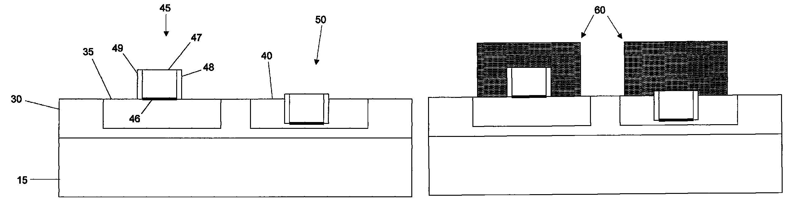
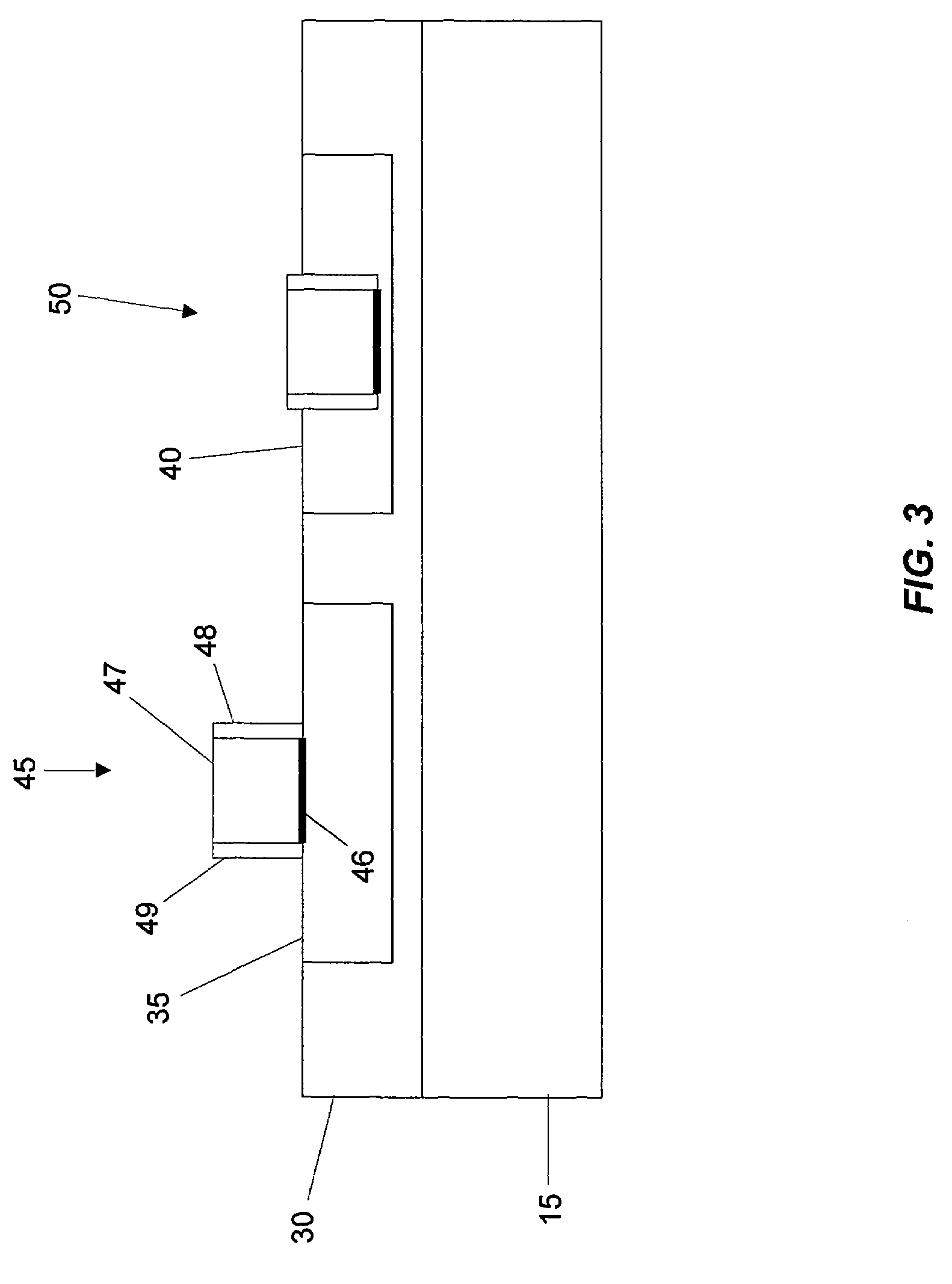
[0017]The invention is directed to semiconductor devices and methods for manufacturing semiconductor devices with improved device performance, and more particularly to dual stress semiconductor devices and methods for manufacturing the same by imposing dual tensile and compressive stresses. At least one implementation of the invention employs thermal oxidation to dually stress opposite portions of silicon-on-insulator (SOI). In this manner, the invention provides improved mobility for NFETs and PFETs.

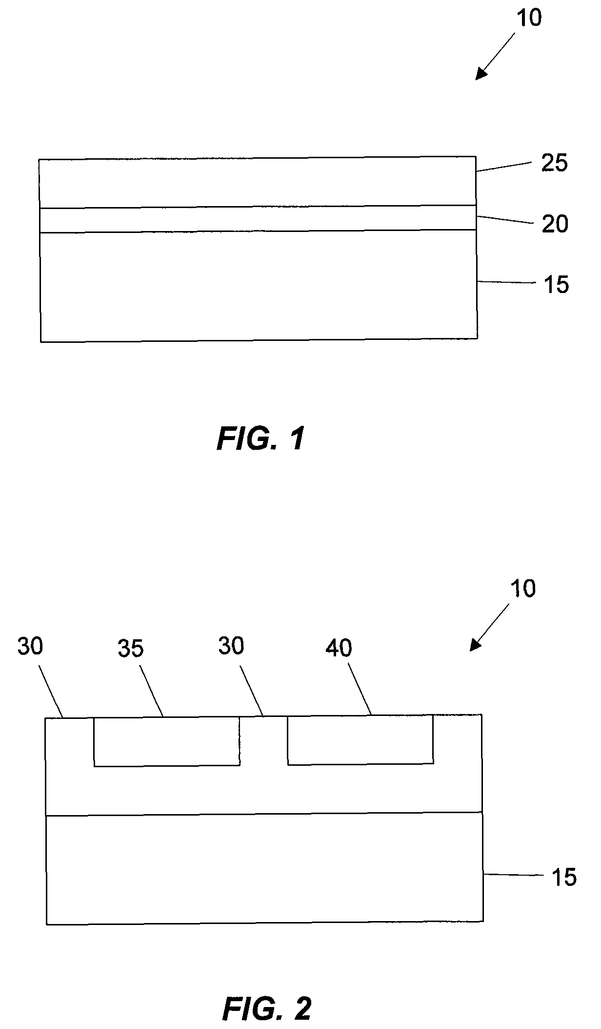
[0018]FIG. 1 shows an exemplary substrate structure 10 employed in the invention. More particularly, a silicon-on-insulator (SOI) type substrate structure is shown, although other substrate structures may be implemented with the invention. The substrate structure 10 has a semiconductor substrate 15, which is typically a silicon substrate, a buried oxide (BOX) layer 20 formed on the substrate 15, and a semiconductor layer 25, which is typically a silicon layer, formed on the buried oxide...


PUM


Abstract

A semiconductor device including semiconductor material having a bend and a trench feature formed at the bend, and a gate structure at least partially disposed in the trench feature. A method of fabricating a semiconductor structure including forming a semiconductor material with a trench feature over a layer, forming a gate structure at least partially in the trench feature, and bending the semiconductor material such that stress is induced in the semiconductor material in an inversion channel region of the gate structure.

Description

FIELD OF THE INVENTION[0001]The invention generally relates to a semiconductor device and methods for manufacturing a semiconductor device with improved device performance, and more particularly to a dual stress semiconductor device and methods for manufacturing the same by imposing dual tensile and compressive stresses.BACKGROUND OF THE INVENTION[0002]Mechanical stresses (e.g., tensile stress and compressive stress) within a semiconductor device can modulate device performance, which means stresses within a semiconductor substrate enhance semiconductor device characteristics. Thus, the characteristics of a semiconductor device can be improved by creating tensile and / or compressive stresses in the channel regions of an N type device (e.g., NFET) and / or a P type device (e.g., PFET). However, the same stress component, either tensile or compressive stress, discriminatively affects the characteristics of an N type device and a P type device. For example, when tensile stress is applied ...

Claims


Application Information

Patent Timeline
Patent Type & Authority Patents(United States)
IPC IPC(8): H01L21/336H01L21/84H01L29/78
CPCH01L21/823807H01L21/823821H01L21/823878H01L27/1203H01L29/1037H01L29/66795H01L29/7843H01L29/7846H01L29/7849H01L29/785H01L21/31155H01L21/76283H01L29/66621H01L21/8238
Inventor ANDERSON, BRENT A.BRYANT, ANDRESNOWAK, EDWARD J.
Owner GLOBALFOUNDRIES INC
Features
  • R&D
  • Intellectual Property
  • Life Sciences
  • Materials
  • Tech Scout
  • Unparalleled Data Quality
  • Higher Quality Content
  • 60% Fewer Hallucinations
Learn More