
Semiconductor device

a technology of semiconductor devices and semiconductors, applied in the direction of semiconductor devices, electrical equipment, plastic recycling, etc., can solve the problems of high switching speed, insufficient isub>ce/sub>, and high isub>ce/sub>, and achieve excellent collector-emitter current characteristics, short fall time, and high latch-up tolerance of parasitic thyristors

Inactive Publication Date: 2010-11-09
ASTRAZENCCA +1
View PDF16 Cites 2 Cited by
  • Summary
  • Abstract
  • Description
  • Claims
  • Application Information

AI Technical Summary

Benefits of technology

The present invention provides a semiconductor device with improved collector-emitter current characteristics, shortened fall time, and increased latch-up tolerance of a parasitic thyristor. The device includes multiple unit semiconductor elements, each containing an IGBT with a unique structure that controls movement of carriers between the collector layer and the emitter layer. This structure allows for better control of current flow and reduces the likelihood of damage from short-circuit events. The invention solves problems associated with conventional IGBTs and provides a more reliable and efficient semiconductor device.

Problems solved by technology

This causes a problem that however high VCE becomes, ICE will not become sufficiently large.
There is another problem that as the gradient expressing ICE remains moderate while VCE grows from 0V to 6V and the ON-resistance (VCE / ICE) is therefore high.
The junction-isolated (JI) horizontal IGBT 700 in which the IGBT is formed in the n− layer 2 on the p-type substrate 1 thus has problem that its switching speed is slow and it has a large switching loss.

Method used


Image

  • Semiconductor device
  • Semiconductor device
  • Semiconductor device

Examples


embodiment 1

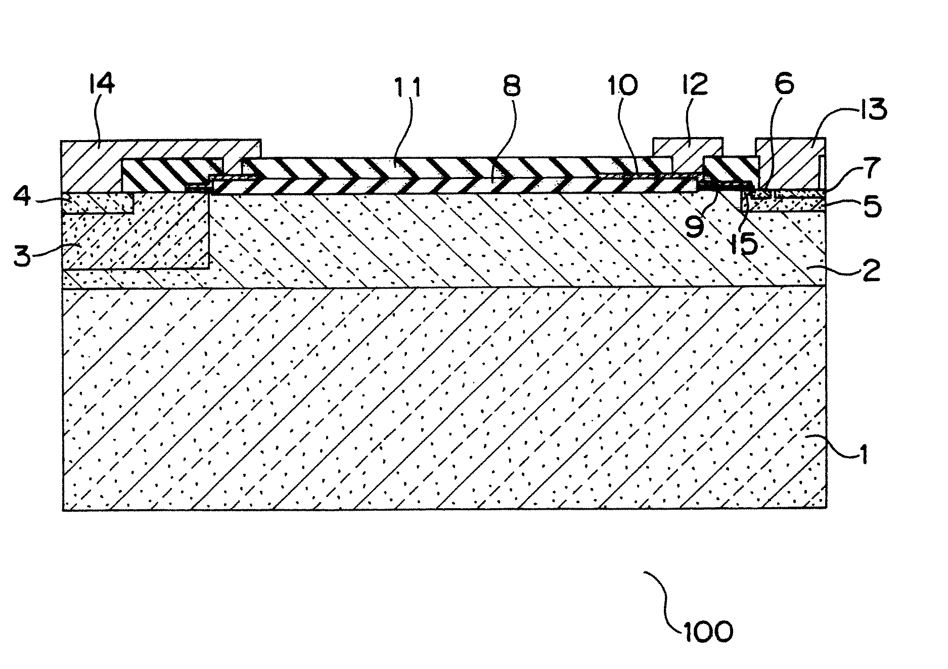
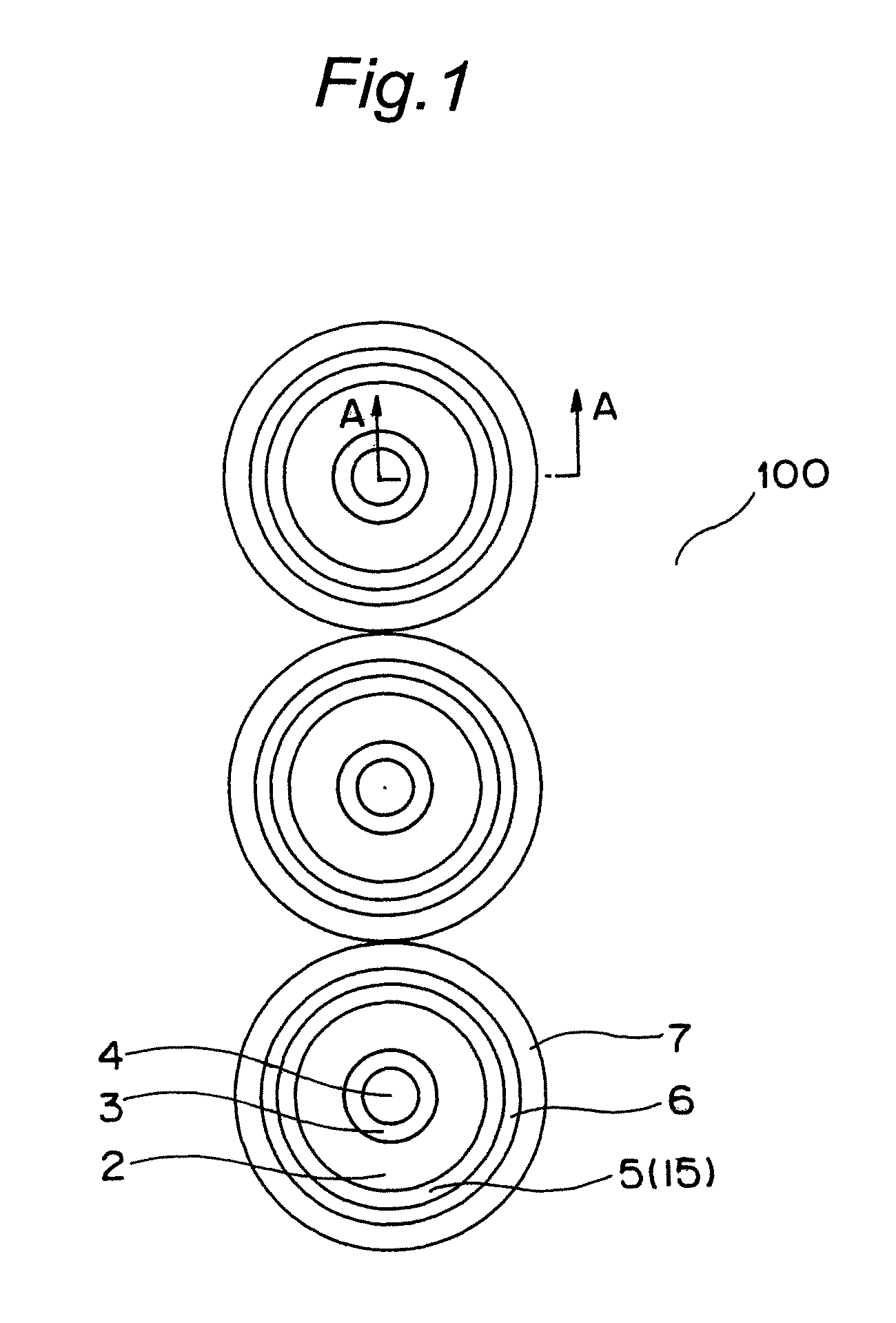
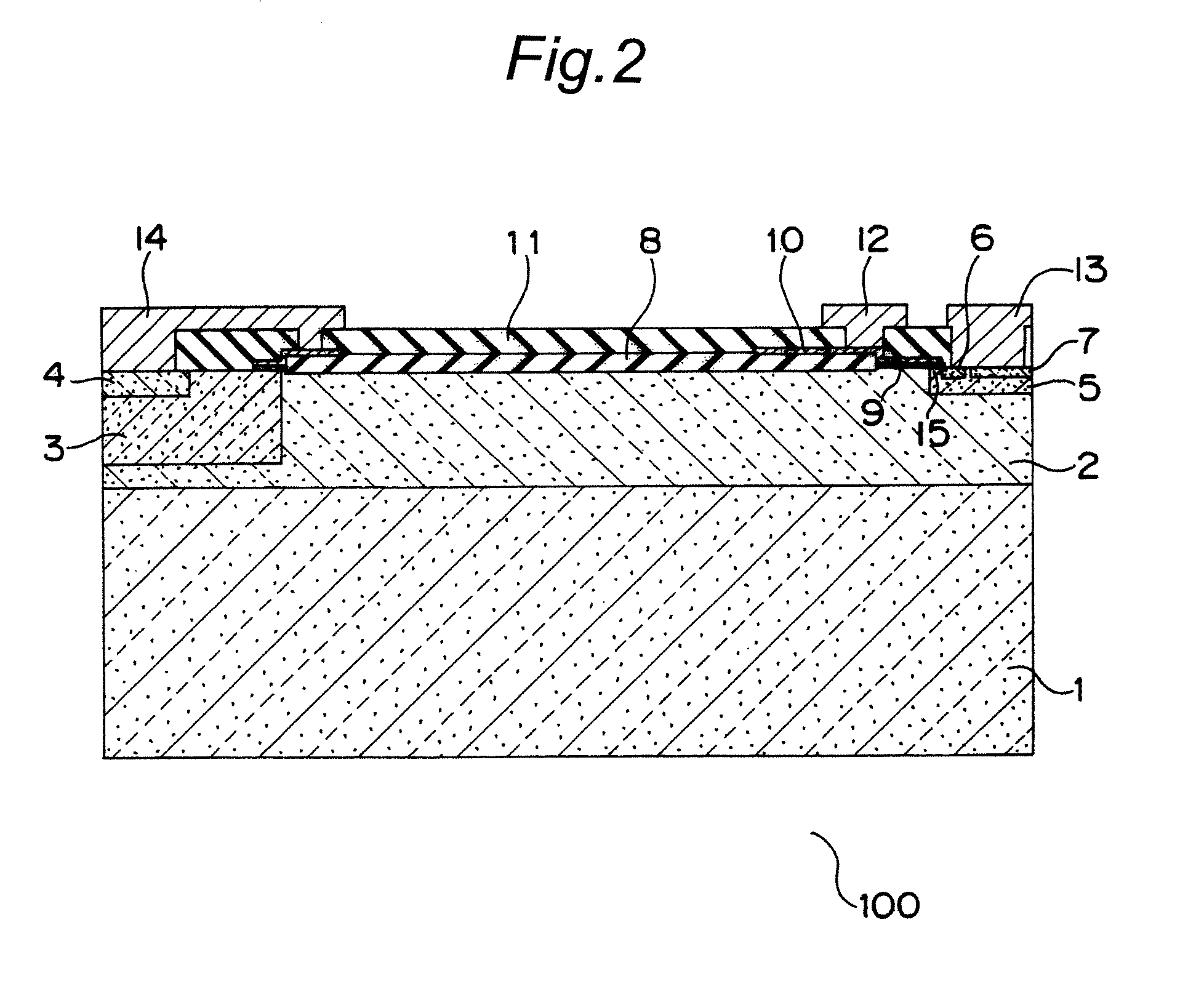
[0077]FIG. 1 is a top view of a horizontal n-channel IGBT (Insulated Gate Bipolar Transistor) according to the embodiment 1 of the present invention generally denoted at 100. FIG. 2 is a cross sectional view of FIG. 1 taken along the direction A-A.

[0078]As shown in FIG. 2, the IGBT 100 includes a p-type substrate 1 of silicon or the like. The p-type substrate 1 seats an n− layer 2 in which an n-type buffer layer 3 is selectively formed. There is a p-type collector layer 4 selectively formed in the n-type buffer layer 3.

[0079]The buffer layer 3 may be omitted (This similarly applies also to the embodiments described below.).

[0080]In the n− layer 2, the p-type base layer 5 is selectively formed in over a predetermined distance from the p-type collector layer 4. In the p-type base layer 5, the n-type emitter layers (n+) 6 are selectively formed so that they are located on the inner side relative to a peripheral portion of the p-type base layer 5 and shallower than the p-type base layer...

embodiment 2

[0096]FIG. 9 is a top view of a horizontal n-channel IGBT according to the embodiment 2 of the present invention generally denoted at 200. FIG. 10 is a cross sectional view of FIG. 9 taken along the direction B-B. In FIGS. 9 and 10, the same reference symbols as those appearing in FIGS. 1 and 2 denote the same or corresponding portions.

[0097]As shown in FIG. 10, the IGBT 200 has an SOI structure in which a buried oxide film 20 which may be a silicon oxide film for example is formed between the p-type substrate 1 and the n− layer 2. The structure is otherwise the same as that of the IGBT 100. The structure of the IGBT 200 shown in the top view in FIG. 9 is the same as the structure of the IGBT 100 shown in FIG. 2. In this structure, the conductivity type of the substrate 1 can be chosen irrespectively of the conductivity type of the n− layer 2.

[0098]FIG. 11 is a top view of another IGBT according to the embodiment 2 of the present invention generally denoted at 250. This is the same ...

embodiment 3

[0117]FIG. 19 is a cross sectional view of a horizontal n-channel IGBT according to the embodiment 3 of the present invention generally denoted at 300, which is illustration viewed from the same direction as the A-A direction in FIG. 1. In FIG. 19, the same reference symbols as those appearing in FIG. 2 denote the same or corresponding portions.

[0118]The IGBT 300 shown in FIG. 19 includes, on the emitter side, a p− layer 30 which is formed narrower and deeper than the p-type base layer 5 but not deep enough to reach the p-type substrate 1 in such a manner that it contacts the bottom surface of the p-type base layer 5. The structure is otherwise the same as that of the IGBT 100 which is shown in FIG. 2.

[0119]FIG. 20 is a cross sectional view of other horizontal n-channel IGBT according to the embodiment 3 of the present invention generally denoted at 350, which is illustration viewed from the same direction as the B-B direction in FIG. 9. In FIG. 20, the same reference symbols as tho...


PUM

PropertyMeasurementUnit
fall timeaaaaaaaaaa
fall timeaaaaaaaaaa
conductivityaaaaaaaaaa

Abstract

A horizontal semiconductor device having multiple unit semiconductor elements, each of said unit semiconductor element formed by an IGBT including: a semiconductor substrate of a first conductivity type; a semiconductor region of a second conductivity type formed on the semiconductor substrate; a collector layer of the first conductivity type formed within the semiconductor region; a ring-shaped base layer of the first conductivity type formed within the semiconductor region such that the base layer is off said collector layer but surrounds said collector layer; and a ring-shaped first emitter layer of the second conductivity type formed in said base layer, wherein movement of carriers between the first emitter layer and the collector layer is controlled in a channel region formed in the base layer, and the unit semiconductor elements are disposed adjacent to each other.

Description

CROSS-REFERENCE TO RELATED APPLICATION[0001]The disclosure of Japanese Patent Applications No. 2005-367544 filed on Dec. 21, 2005 and No. 2006-98740 filed on Mar. 31, 2006 including specification, drawings and claims are incorporated herein by reference in its entirely.BACKGROUND OF THE INVENTION[0002]1. Field of the InventionTechnical Field[0003]The present invention relates to a semiconductor device, and more particularly, to a high-voltage power semiconductor device.[0004]2. Description of the Related ArtBackground Art[0005]FIG. 49 is a top view of a conventional horizontal n-channel IGBT (Insulated Gate Bipolar Transistor) generally denoted at 700. FIG. 50 is a cross sectional view of FIG. 49 taken along the direction X-X.[0006]As shown in FIG. 50, the IGBT 700 includes a p-type substrate 1. The p-type substrate 1 seats an n− layer 2 in which an n-type buffer layer 3 is formed. There is a p-type collector layer 4 in the n-type buffer layer 3.[0007]A p-type base layer 5 is formed...

Claims


Application Information

Patent Timeline
Patent Type & Authority Patents(United States)
IPC IPC(8): H01L29/76
CPCH01L29/0696H01L29/7393H01L29/7394H01L27/088B29K2105/26Y02W30/62
Inventor HATADE, KAZUNARI
Owner ASTRAZENCCA
Learn More