

Semiconductor device
a technology of semiconductors and semiconductors, applied in the field of high-voltage power semiconductor devices, can solve the problems of high resistance (vce/ice), insufficient ice, and slow switching speed, and achieve the effects of excellent collector-emitter current characteristics, high latch-up tolerance of parasitic thyristors, and short fall tim
- Summary
- Abstract
- Description
- Claims
- Application Information
AI Technical Summary
Benefits of technology
Problems solved by technology
Method used
Image

Examples
embodiment 1
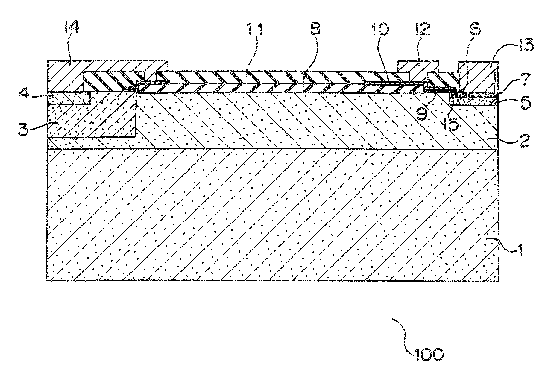
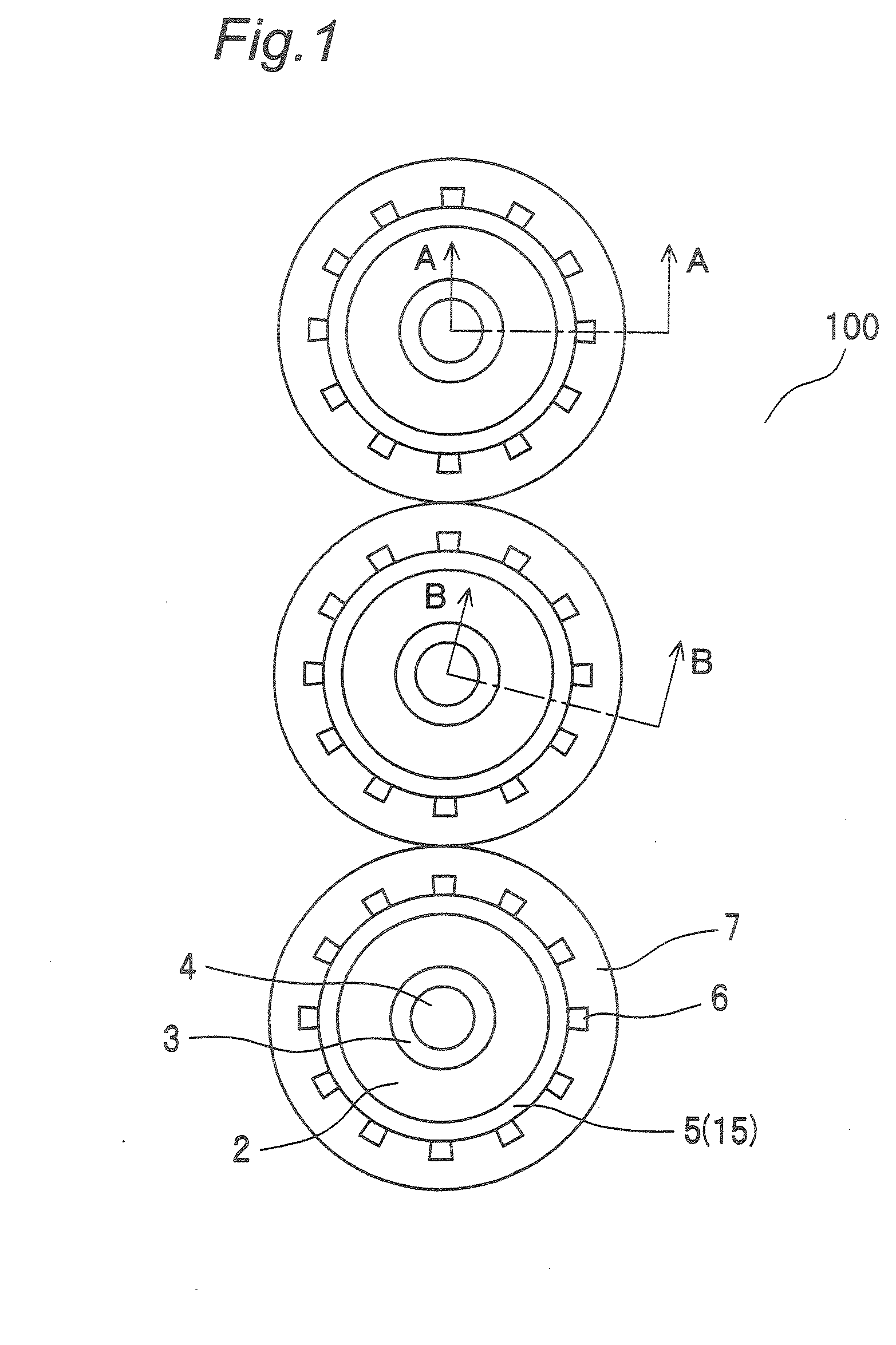
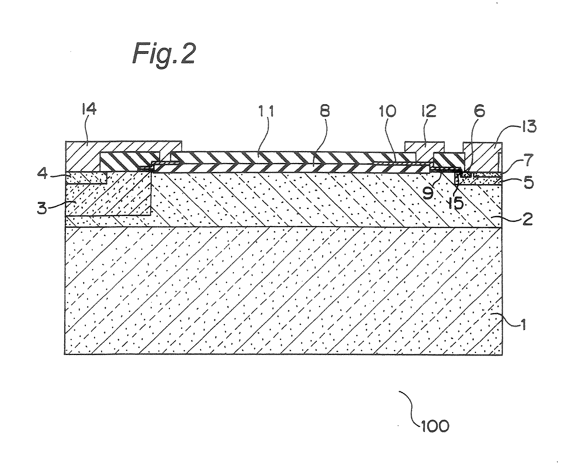
[0053]FIG. 1 is a top view of a horizontal n-channel IGBT (Insulated Gate Bipolar Transistor) according to the Embodiment 1 of the present invention generally denoted at 100. FIG. 2 is a cross sectional view of FIG. 1 taken along the direction A-A, while FIG. 3 is a cross sectional view of FIG. 1 taken along the direction B-B.
[0054]As shown in FIG. 1, multiple circular unit IGBTs are disposed next to each other in the IGBT 100 (In FIG. 1, there are three unit IGBTs.). In each unit IGBT, a p-type collector layer 4 is located at the center, and an n-type buffer layer 3, an n− layer 2 and a p-type base layer 5 are disposed in an approximately concentric arrangement around the p-type collector layer 4. Disposed around the p-type base layer 5 are plural n-type emitter layers (unit emitter layers) 6 which are shaped like stripes in such a manner that the n-type emitter layers are apart from each other in an approximately concentric arrangement, and the p-type base layer 5 located between ...
embodiment 2
[0084]FIGS. 14 and 15 are cross sectional views of an IGBT according to the Embodiment 2 of the present invention generally denoted at 400, which respectively correspond to a cross sectional view taken along the direction A-A shown in FIG. 1 and a cross sectional view taken along the direction B-B shown in FIG. 1.
[0085]The IGBT 400 has an SOI structure (of the dielectric-isolated horizontal type) in which a buried oxide film 20 which may be a silicon oxide film for example is formed between the p-type substrate 1 and the n− layer 2. The structure is otherwise the same as that of the IGBT 100 (which is of the junction-isolated horizontal type) (See FIGS. 2 and 3.).
[0086]FIGS. 16 and 17 are cross sectional views of other IGBTs according to the Embodiment 2 of the present invention generally denoted at 500, which respectively correspond to a cross sectional view taken along the direction A-A shown in FIG. 5 and a cross sectional view taken along the direction B-B shown in FIG. 5.
[0087]...
embodiment 3
[0090]FIG. 18 is a cross sectional view of an IGBT according to the Embodiment 3 of the present invention generally denoted at 600, taken along the direction A-A shown in FIG. 1. In FIG. 18, the same reference numerals as those appearing in FIG. 2 denote the same or corresponding portions.
[0091]The IGBT shown in FIG. 18 includes, on the emitter side, a p− layer 30 which is formed narrower and deeper than the p-type base layer 5 but not deep enough to reach the p-type substrate 1 in such a manner that it contacts the bottom surface of the p-type base layer 5. The structure is otherwise the same as that of the IGBT 100 which is shown in FIG. 2.
[0092]FIG. 19 is a cross sectional view of another IGBT according to the Embodiment 3 of the present invention generally denoted at 600, also taken along the direction A-A shown in FIG. 1. The IGBT 700 has an SOI structure (of the dielectric-isolated horizontal type) which is the same as the structure of the IGBT 600 as it is modified to include...
PUM
 Abstract
Description
Claims
Application Information