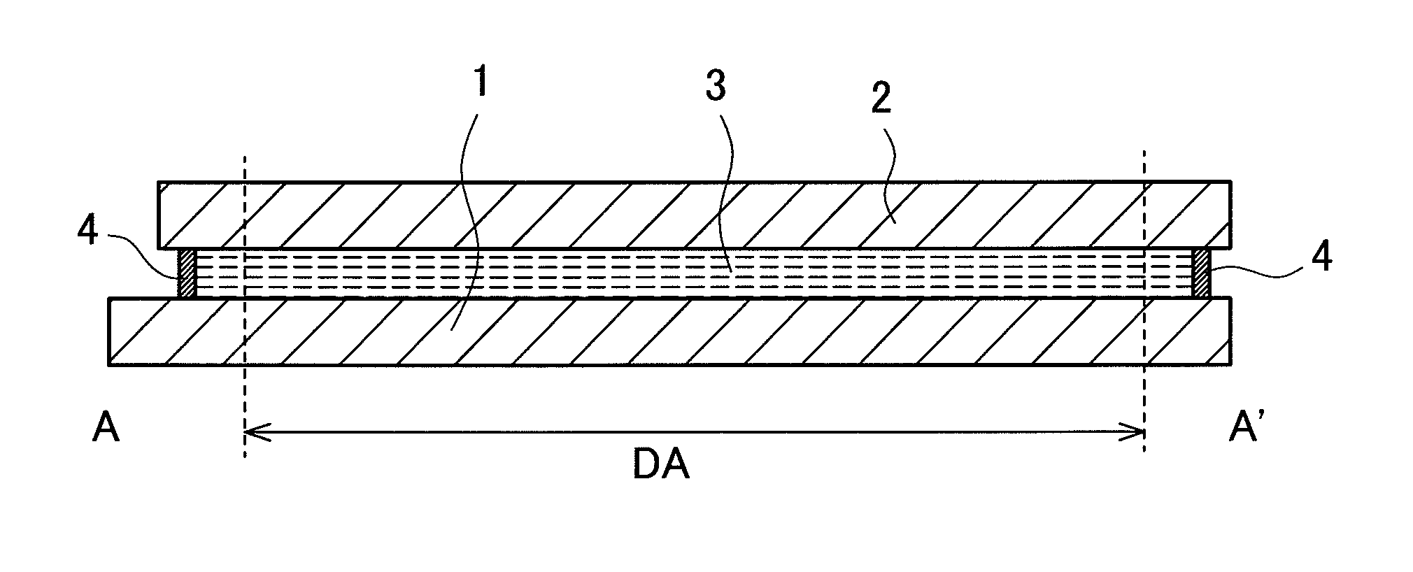
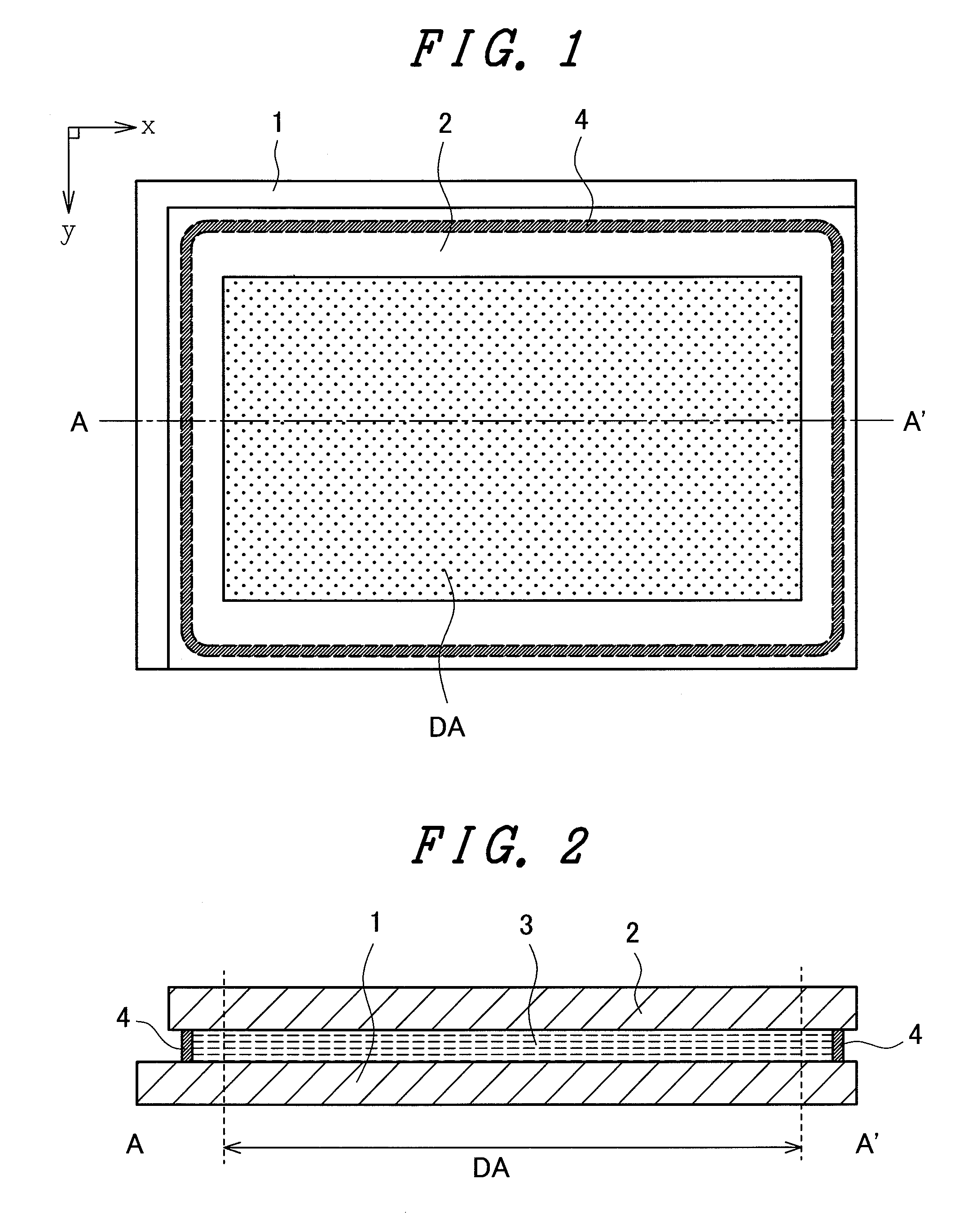
Display device

a technology of a display device and a pixel electrode, which is applied in the direction of non-linear optics, instruments, optics, etc., can solve the problems of fine recessed defects, light leakage, and conductive failure between the source electrode and the pixel electrode of the tft substra

Active Publication Date: 2010-11-23
PANASONIC INTELLECTUAL PROPERTY CORP OF AMERICA +1
View PDF7 Cites 2 Cited by
  • Summary
  • Abstract
  • Description
  • Claims
  • Application Information

AI Technical Summary

Benefits of technology

[0013]Accordingly, it is an object of the present invention to provide a technique which can reduce a connection failure between two conductive layers which are connected with each other via a through hole in a display device.
[0014]It is another object of the present invention to provide, for example, a technique which is capable of reducing a connection failure between a source electrode of a TFT element and a pixel electrode which are connected with each other via a through hole in a liquid crystal display device.
[0015]It is another object of the present invention to provide, for example, a technique which can reduce a defect of an orientation film formed on a TFT substrate side in the liquid crystal display device.
[0020]In the display device of the present invention, due to the characterizing constitution thereof, for example, in forming the second conductive layer by etching, the resist material in a liquid form which is applied to the conductive film by printing or coating easily enters a recessed portion formed in the opening portion thus preventing a shape defect of an etching resist. Accordingly, it is possible to prevent a conductive failure between the first conductive film and the second conductive film in the opening portion.
[0023]The substrate of the liquid crystal display panel forms an orientation film on an interface thereof with the liquid crystal material (liquid crystal layer) and the orientation film is formed by applying a resin material in a liquid form to a surface of the substrate in which a recessed portion is formed by the opening portion (through hole) by printing or coating. Accordingly, by changing a distance between an outer periphery of the opening end remoter from the surface of the substrate in distance and the surface of the substrate, for example, the printed resin material in a liquid form can easily enter the recessed portion formed in the opening portion thus preventing a shape defect of the orientation film.
[0026]Further, in the display panel such as a liquid crystal display panel, for example, the TFT element adopts various constitutions (structures). Besides the above-mentioned combination of the source electrode and the pixel electrode and the combination of the common electrode and the bridge line, other conductive layers may be connected via the opening portion (through hole). Also in such a case, by providing the above-mentioned constitution to the opening portion, when a material in a liquid form is applied to the second conductive layer by printing or coating, the printed material in a liquid form can easily enter the recessed portion formed in the opening portion.

Problems solved by technology

As a result, for example, there arises a drawback that a conductive failure is generated between the source electrode and the pixel electrode of the TFT substrate.
Accordingly, there have been drawbacks that fine recessed defects are generated in the orientation film on the TFT substrate side, the orientation irregularities occur in the through hole portion, and leaking of light occurs.

Method used


Image

  • Display device
  • Display device
  • Display device

Examples


embodiment 1

[0075]FIG. 6 and FIG. 7 are schematic views showing the schematic constitution of an essential part of the liquid crystal display panel of the embodiment 1 according to the present invention.

[0076]FIG. 6 is a schematic plan view showing the schematic constitution of the through hole of the embodiment 1, and FIG. 7 is a schematic cross-section al view taken along a line D-D′ in FIG. 6.

[0077]This embodiment 1 focuses on the through hole which connects the source electrode of the TFT element and the pixel electrode and the constitution al example to which the present invention is applied and the manner of operation and advantageous effects of the constitution al example are explained.

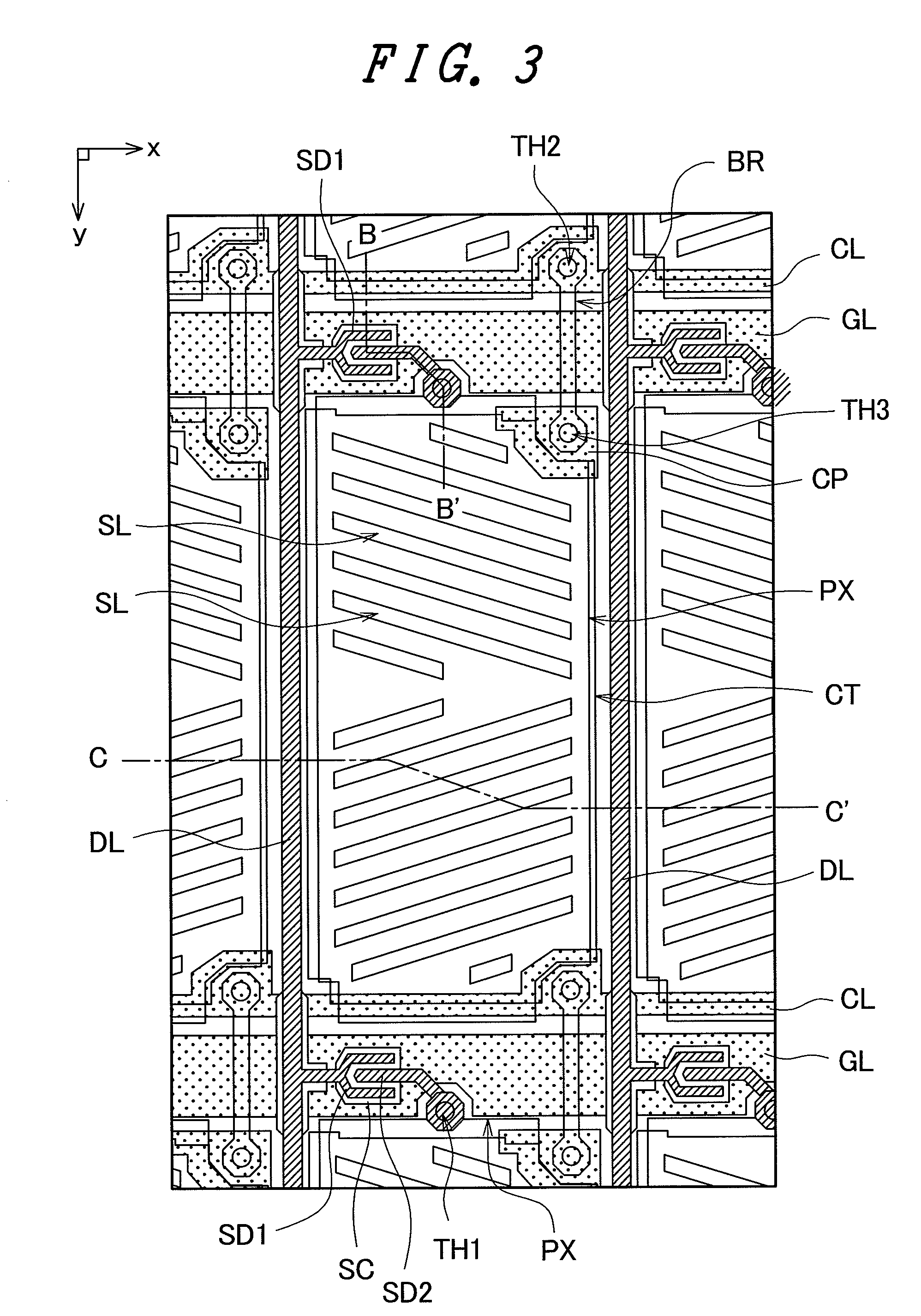
[0078]When one pixel of the display region DA adopts the constitution shown in FIG. 3 to FIG. 5, by applying the present invention to the connection portion between the source electrode SD2 of the TFT element and the pixel electrode PX, it is possible to achieve the constitution shown in FIG. 6 and FIG. 7,...

embodiment 2

[0098]FIG. 18 and FIG. 19 are schematic views showing the schematic constitution of an essential part of a liquid crystal display panel of an embodiment 2 according to the present invention.

[0099]FIG. 18 is a schematic plan view showing the schematic constitution of a through hole in the embodiment 2. FIG. 19 is a schematic cross-section al view taken along a line H-H′ in FIG. 18.

[0100]In the embodiment 1, by focusing on the through hole which connects the source electrode of the TFT element and the pixel electrode, as the constitution al example to which the present invention is applied, the case which provides the stepped-portion forming layer MR is exemplified. Further, by allowing the outer periphery AR of the opening end of the through hole (opening hole) TH1 formed in the second insulation layer PAS2 remote from the glass substrate SUB to pass through the region where the stepped-portion forming layer MR is provided and the region where the stepped-portion forming layer MR is ...

embodiment 3

[0106]FIG. 20 and FIG. 21 are schematic views showing the schematic constitution of an essential part of a liquid crystal display panel of an embodiment 3 according to the present invention.

[0107]FIG. 20 is a schematic plan view showing the schematic constitution of a through hole in the embodiment 3. FIG. 21 is a schematic cross-section al view taken along a line J-J′ in FIG. 20.

[0108]In the embodiment 1 and the embodiment 2, as one example of the through hole formed in the TFT substrate 1 of the liquid crystal display panel, the through hole TH1 which connects the source electrode SD2 and the pixel electrode PX is exemplified. However, one pixel adopts the pixel constitution of the TFT substrate having the constitution shown in FIG. 3 to FIG. 5, besides the through hole TH1, the through hole TH2 which connects the bridge line BR and the common signal line CL and the like may be formed, for example.

[0109]The embodiment 3 focuses on the through hole TH2 which connects the bridge lin...


PUM

PropertyMeasurementUnit
transparentaaaaaaaaaa
conductiveaaaaaaaaaa
distanceaaaaaaaaaa

Abstract

The present invention reduces a connection failure between two conductive layers which are connected with each other via a through hole in a display device and reduces a defect of an orientation film formed on a TFT substrate side in a liquid crystal display device. A display device includes a display panel in which a first conductive layer formed on a surface of a substrate, and a second conductive layer which is formed over the first conductive layer as viewed from a surface of the substrate by way of a thin film layer formed of one insulation film or two or more stacked thin films including one insulation film are electrically connected with each other in an opening portion formed in the thin film layer. Out of opening ends of the opening portion of the thin film layer, an outer periphery of the opening end remote from the surface of the substrate changes a distance from the surface of the substrate one time or more during one turn of the outer periphery.

Description

[0001]The present application claims priority from Japanese application JP2006-150773 filed on May 31, 2006, the content of which is hereby incorporated by reference into this application.BACKGROUND OF THE INVENTION[0002]1. Field of the Invention[0003]The present invention relates to a display device, and more particularly to a technique which is effectively applicable to through holes formed in a display region of a liquid crystal display device.[0004]2. Description of the Related Art[0005]Convention ally, as a display device which displays a video or an image, there has been known a liquid crystal display device which uses a liquid crystal display panel sealing a liquid crystal material between a pair of substrates.[0006]In the liquid crystal display panel, one substrate out of a pair of substrates is generally referred to as a TFT substrate, and on a surface of a transparent substrate, a plurality of scanning signal lines and a plurality of video signal lines which stereoscopical...

Claims


Application Information

Patent Timeline
Patent Type & Authority Patents(United States)
IPC IPC(8): G02F1/1343
CPCG02F1/136227G02F1/1309G02F2001/136272G02F2001/13629G02F1/136272G02F1/13629
Inventor IWATO, HIROAKIARAYA, KOTAROTERADA, KENJI
Owner PANASONIC INTELLECTUAL PROPERTY CORP OF AMERICA
Why Eureka
Try Eureka