Deposition of electronic circuits on fibers and other materials

a technology of electronic circuits and fibers, applied in vacuum evaporation coatings, heat inorganic powder coatings, sputtering coatings, etc., can solve the problems of inconvenient transportation of even a single portable electronic device, insufficient storage or attachment of the portable electronic device itself, and the weight of the portable device itsel

Inactive Publication Date: 2010-12-07
NIKE INC
View PDF17 Cites 62 Cited by
  • Summary
  • Abstract
  • Description
  • Claims
  • Application Information

AI Technical Summary

Problems solved by technology

Even with additional or specialized pockets, however, transporting even a single portable electronic device may be inconvenient for a user.
A runner or biker may prefer to use streamlined, form fitting clothing in order to improve his or her athletic performance, which may not provide an adequate location for storing or attaching a portable electronic device.
In addition, the weight of the portable device itself, although relatively light, may still be bulky or uncomfortable for the user.
While these techniques offer a variety of advantages over the conventional packaging of portable electronic components into a single, centralized hand-sized container, they still have a number of limitations.

Method used


Image

  • Deposition of electronic circuits on fibers and other materials
  • Deposition of electronic circuits on fibers and other materials
  • Deposition of electronic circuits on fibers and other materials

Examples


Embodiment Construction

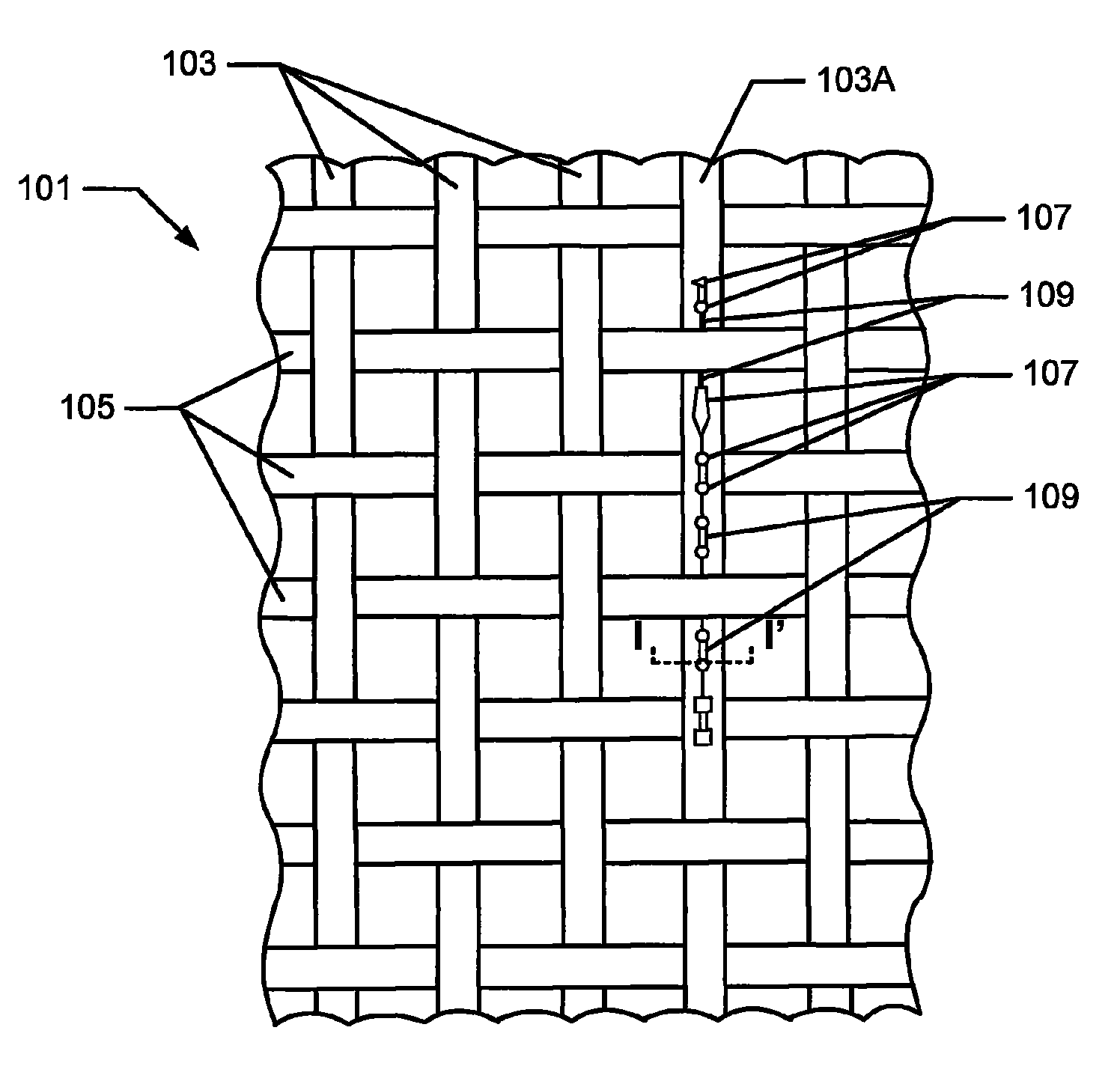
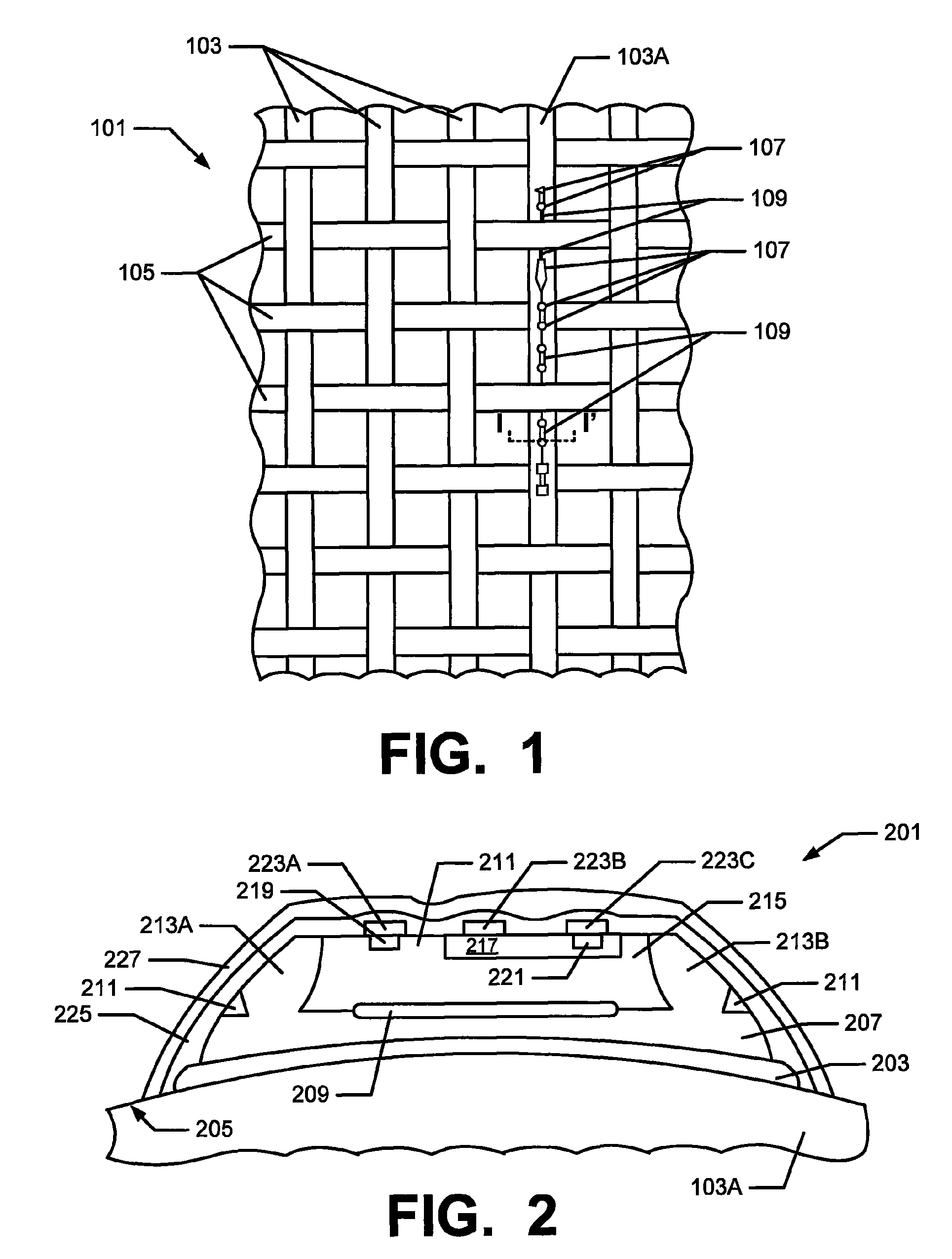
[0013]FIG. 1 illustrates a textile material according to one embodiment of the invention. In this figure, a piece of woven fabric 101 includes warp fibers 103 and weft fibers 105. The fibers 103 and 105 may be any fibrous material suitable for forming wearable items. For example, one or more of fibers 103 and 105 may be natural fibers, such as cotton, wool, silk, or leather. One or more of fibers 103 and 105 may also be formed of any inorganic material suitable for weaving a fabric, such as, e.g., polyester, nylon, polypropylene, or rayon. Of course, the specific fiber materials listed above are for exemplary purposes only and should not be considered limiting.

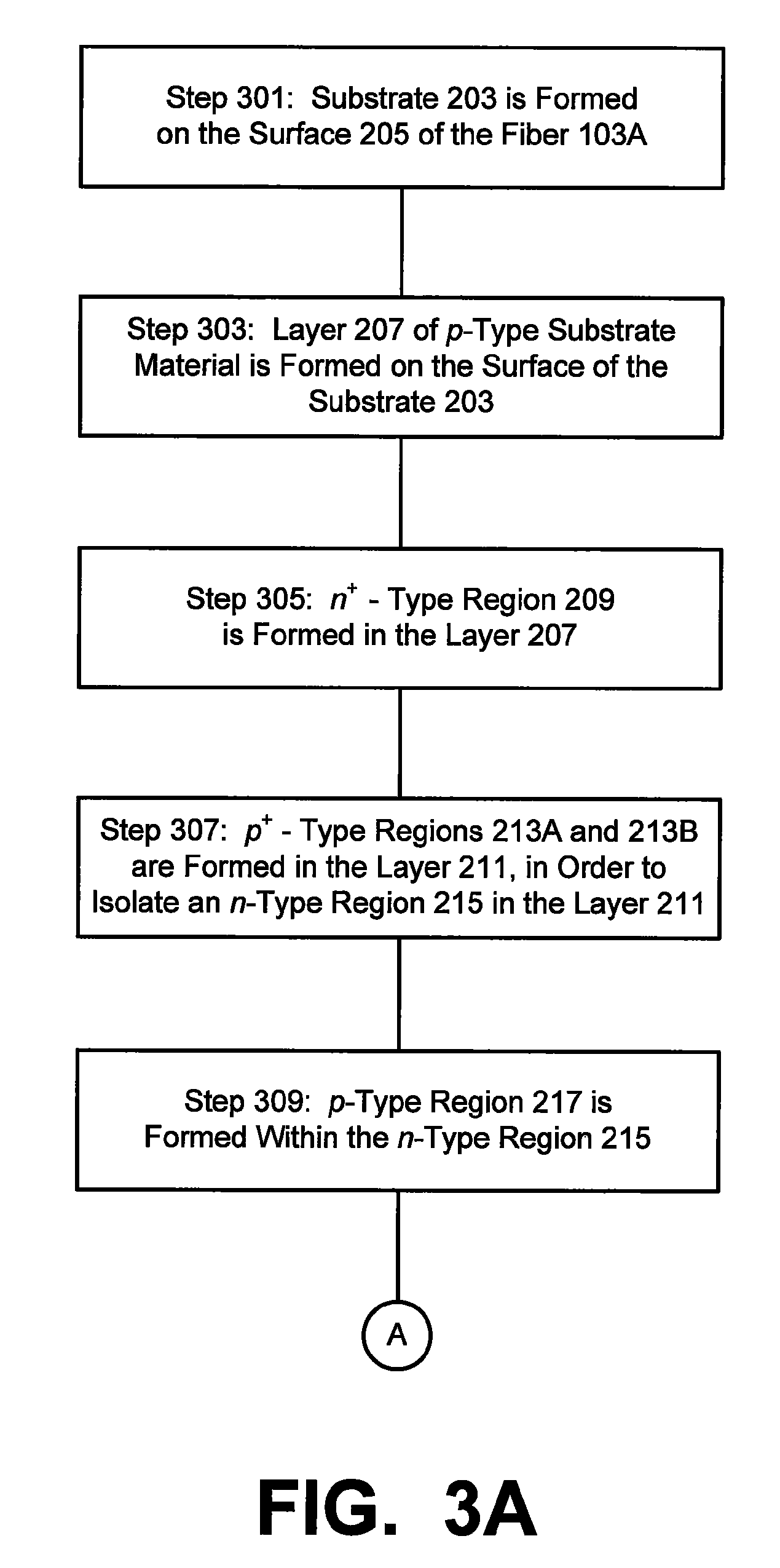
[0014]As illustrated in FIG. 1, the warp fiber 103A has a number of electrical components 107 formed thereon. As will be explained in detail below, the electrical components 107 may be any type of structure that can be formed using conventional integrated circuit fabrication techniques. The electrical components 107 may be, fo...


PUM

PropertyMeasurementUnit
diametersaaaaaaaaaa
diametersaaaaaaaaaa
speedaaaaaaaaaa

Abstract

Fibers, such as textile fibers, having electrical components deposited thereon. More particularly, one or more electrical components are formed directly onto the surface of at least one fiber. The fiber having the electrical component formed thereon may then be interlaced with other fibers to form a larger piece of fabric, which can be employed to produce an article of clothing. A group of transistors and piezoelectric components forming an accelerometer may be woven onto one or more natural or synthetic fibers. The fibers may then be employed as the warp, weft, or both, of a woven piece of fabric, or used to form a knitted piece of fabric. The fabric piece can then be cut and sewn to form a wearable item, such as a shirt, a pair of pants, a hat, or the upper piece of a shoe that includes the accelerometer.

Description

RELATED APPLICATION DATA[0001]This application is a continuation of U.S. patent appln. Ser. No. 10 / 077,548 filed Feb. 14, 2002 in the name of Swatee N. Surve and entitled “Deposition of Electronic Circuits on Fibers and Other Materials.” This priority application is entirely incorporated herein by reference.FIELD OF THE INVENTION[0002]The invention relates to the formation of electrical circuits on the surface of a fiber or other substrate material used to form an article of wear, such as clothing or shoes.BACKGROUND OF THE INVENTION[0003]Electrical devices are becoming ubiquitous in our society. People of all ages, from school children to senior citizens, regularly employ a variety of portable electronic devices. These devices include, for example, personal digital assistants, wireless telephones, and MP3 players. These portable devices also include time and athletic performance measurement devices, such as watches that monitor a wearer's heart rate, distance traveled, and speed. T...

Claims


Application Information

Patent Timeline
Patent Type & Authority Patents(United States)
IPC IPC(8): A41D27/02A41D27/00H05B11/00
CPCA61B5/6804C23C4/04C23C24/08D02G3/00D03D1/0088D03D15/00D03D15/005D06M10/005D06M10/06H01L29/0657H01L29/7317H01Q1/273H05K1/16A41D1/002A61B2562/0219D10B2201/02D10B2201/24D10B2211/02D10B2211/04D10B2321/022D10B2331/02D10B2331/04D10B2401/18D10B2501/00D10B2501/042D10B2501/043H01L27/12H05K1/00H05K1/038H05K2201/029Y10S2/905Y10T442/40Y10T428/249921Y10T442/30Y10T428/249953
Inventor SWATEE, SURVE N.
Owner NIKE INC
Why Eureka
Try Eureka