
Low-profile connector assembly and methods

a low-profile, connector technology, applied in the direction of contact member manufacturing, coupling device connection, coupling protective earth/shielding arrangement, etc., can solve the problem of tended to be unsuitable for further miniaturization, and achieve the effect of improving the emi performance of the connector assembly

Active Publication Date: 2010-12-07
PULSE ELECTRONICS
View PDF21 Cites 32 Cited by
  • Summary
  • Abstract
  • Description
  • Claims
  • Application Information

AI Technical Summary

Benefits of technology

The solution effectively reduces EMI emissions, increases port density, and supports higher data rates while conforming to existing standards, such as the SFP standard, by integrating EMI tabs and alignment features within a compact design.

Problems solved by technology

Although past conventional pluggable designs have been used successfully in the past, they have tended to be unsuitable for further miniaturization, an ever-constant objective in the telecommunications industry.
Miniaturizing a module while maintaining or increasing its operating speed presents a number of design problems.

Method used


Image

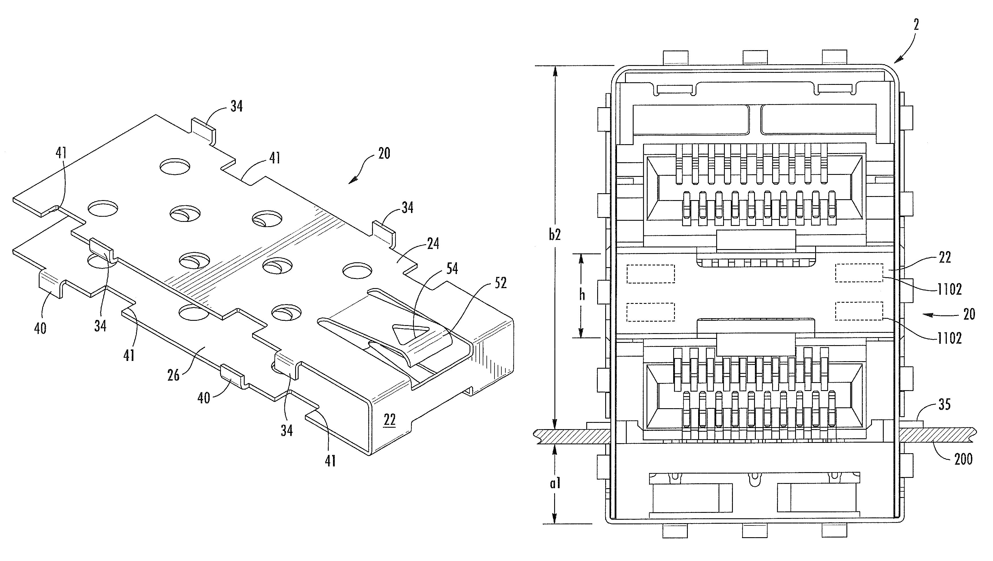
  • Low-profile connector assembly and methods
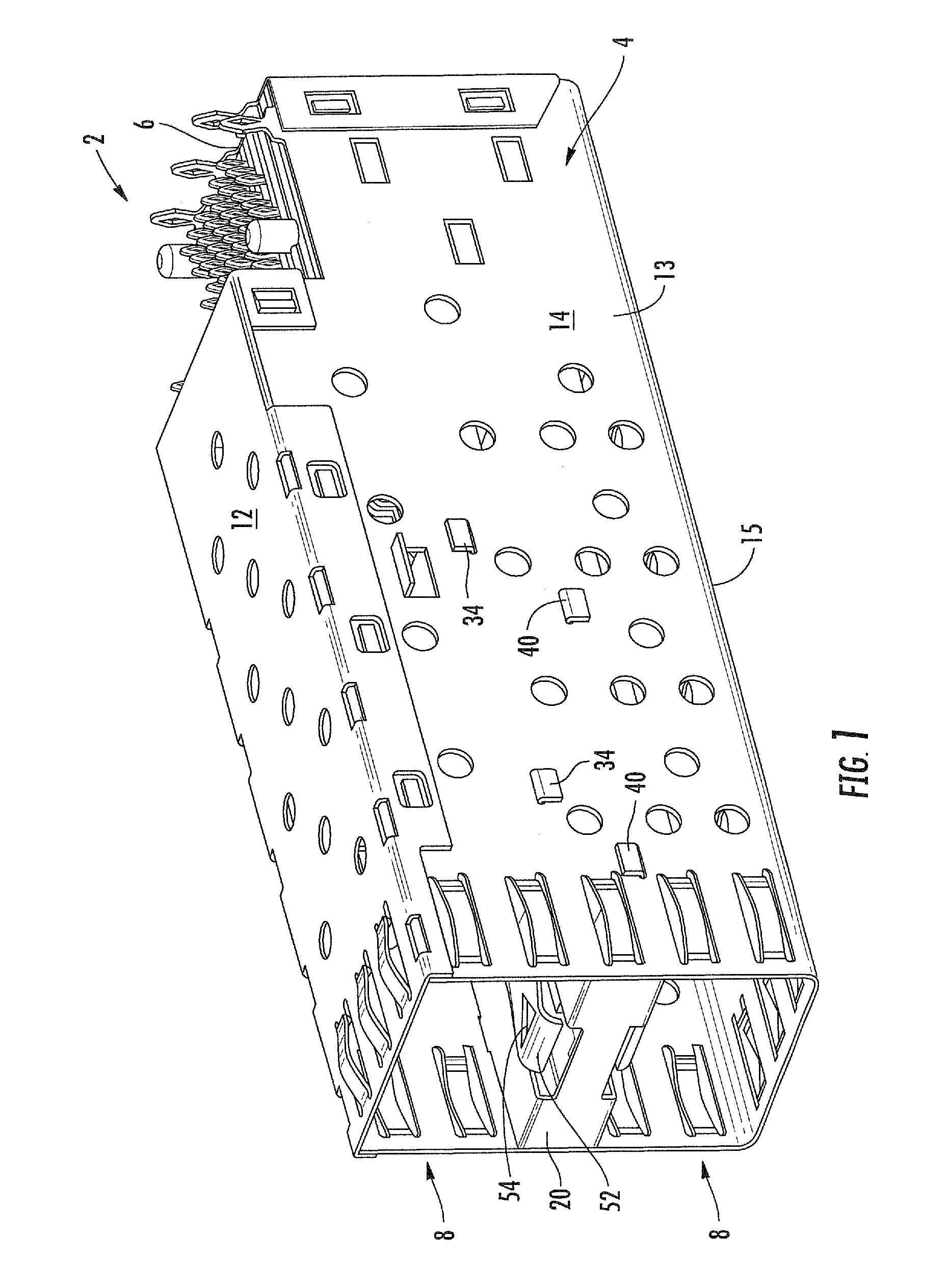
  • Low-profile connector assembly and methods
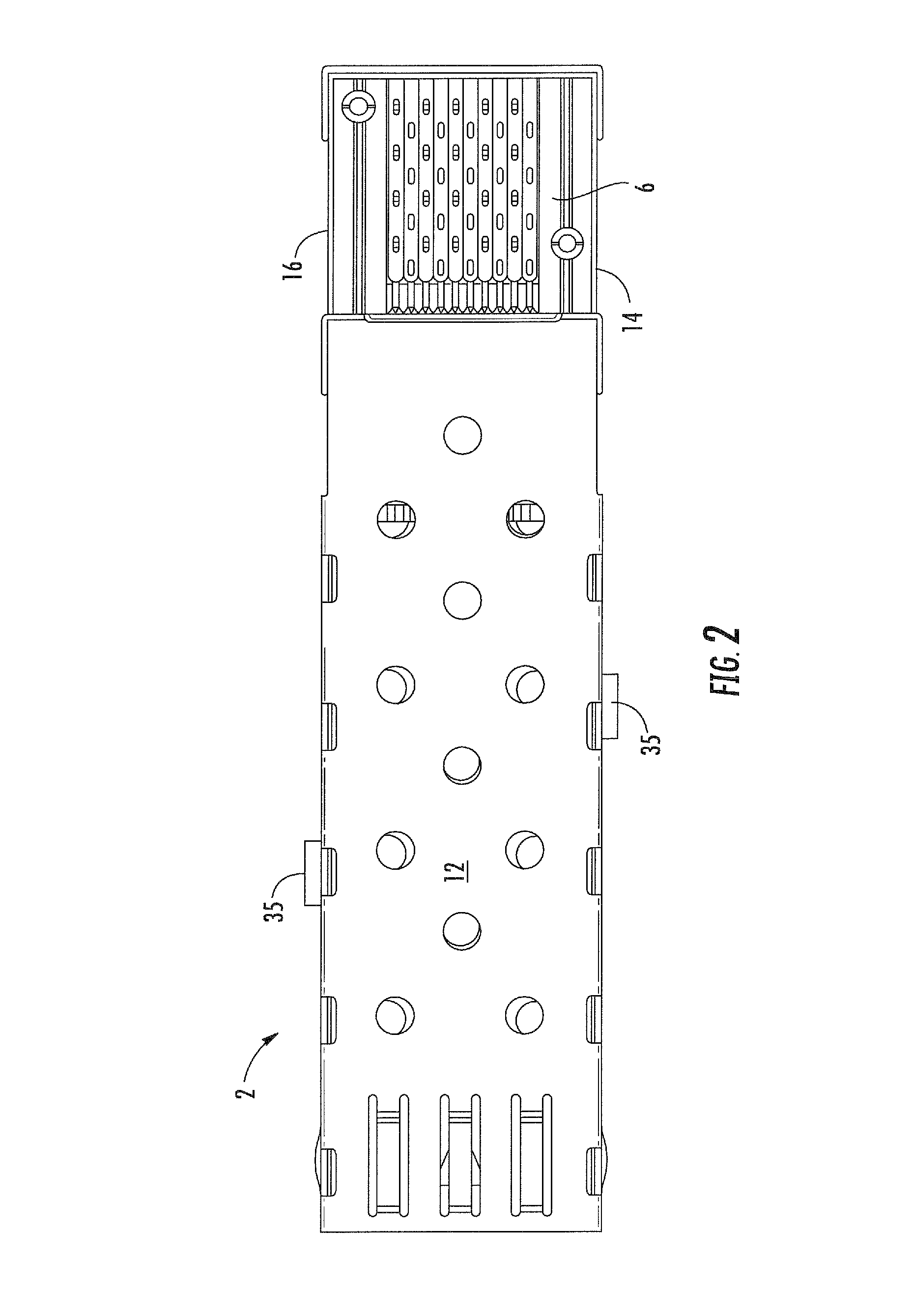
  • Low-profile connector assembly and methods

Examples


Embodiment Construction

[0059]Reference is now made to the drawings wherein like numerals refer to like parts throughout.

[0060]As used herein, the term “integrated circuit (IC)” refers to without limitation any type of device, whether single or multiple die, having any level of integration (including without limitation ULSI, VLSI, and LSI) and irrespective of process or base materials (including, without limitation Si, SiGe, CMOS and GaAs). ICs may include, for example, memory devices (e.g., DRAM, SRAM, DDRAM, EEPROM / Flash, ROM), digital processors, SoC devices, FPGAs, ASICs, ADCs, DACs, transceivers, memory controllers, and other devices, as well as any combinations thereof.

[0061]As used herein, the term “memory” includes any type of integrated circuit or other storage device adapted for storing digital data including, without limitation, ROM. PROM, EEPROM, DRAM, SDRAM, DDR / 2 SDRAM, EDO / FPMS, RLDRAM, SRAM, “flash” memory (e.g., NAND / NOR), and PSRAM.

[0062]As used herein, the terms “microprocessor” and “dig...


PUM

PropertyMeasurementUnit
distanceaaaaaaaaaa
speedaaaaaaaaaa
conductiveaaaaaaaaaa

Abstract

An electrical connector assembly having shielded cage assembly with a plurality of ports for receiving modules. In one embodiment, the modules comprise SFP (small form-factor pluggable) modules, and the electrical connector assembly is adapted for low-profile applications, thereby optimizing the amount of area and volume occupied by the SFP assembly. In one variant, the SFP modules are pluggable into individual ports, whereby two modules are interconnected to a single header connector interconnected to a motherboard. Methods of manufacturing the connector assembly are also disclosed.

Description

PRIORITY[0001]This application claims priority to U.S. Provisional Patent Application Ser. No. 60 / 898,677 filed Jan. 30, 2007 of the same title, which is incorporated herein by reference in its entirety.COPYRIGHT[0002]A portion of the disclosure of this patent document contains material that is subject to copyright protection. The copyright owner has no objection to the facsimile reproduction by anyone of the patent document or the patent disclosure, as it appears in the Patent and Trademark Office patent files or records, but otherwise reserves all copyright rights whatsoever.FIELD OF THE INVENTION[0003]The present invention relates generally to electrical or electronic connector systems and in one exemplary aspect, to low-profile connector systems for pluggable electronic modules, such as transceiver modules for high-speed fiber optic and copper communications, and methods for manufacturing the same.DESCRIPTION OF RELATED TECHNOLOGY[0004]Small form-factor pluggable (“SFP”) optical...

Claims


Application Information

Patent Timeline
Patent Type & Authority Patents(United States)
IPC IPC(8): H01R13/60
CPCH01R23/6873H05K9/0058Y10T29/49204Y10S439/939H01R12/727H01R13/658H01R25/006
Inventor CHENG, YICANJUNG, TSOU CHENGJACKSON, MARK
Owner PULSE ELECTRONICS
Learn More