

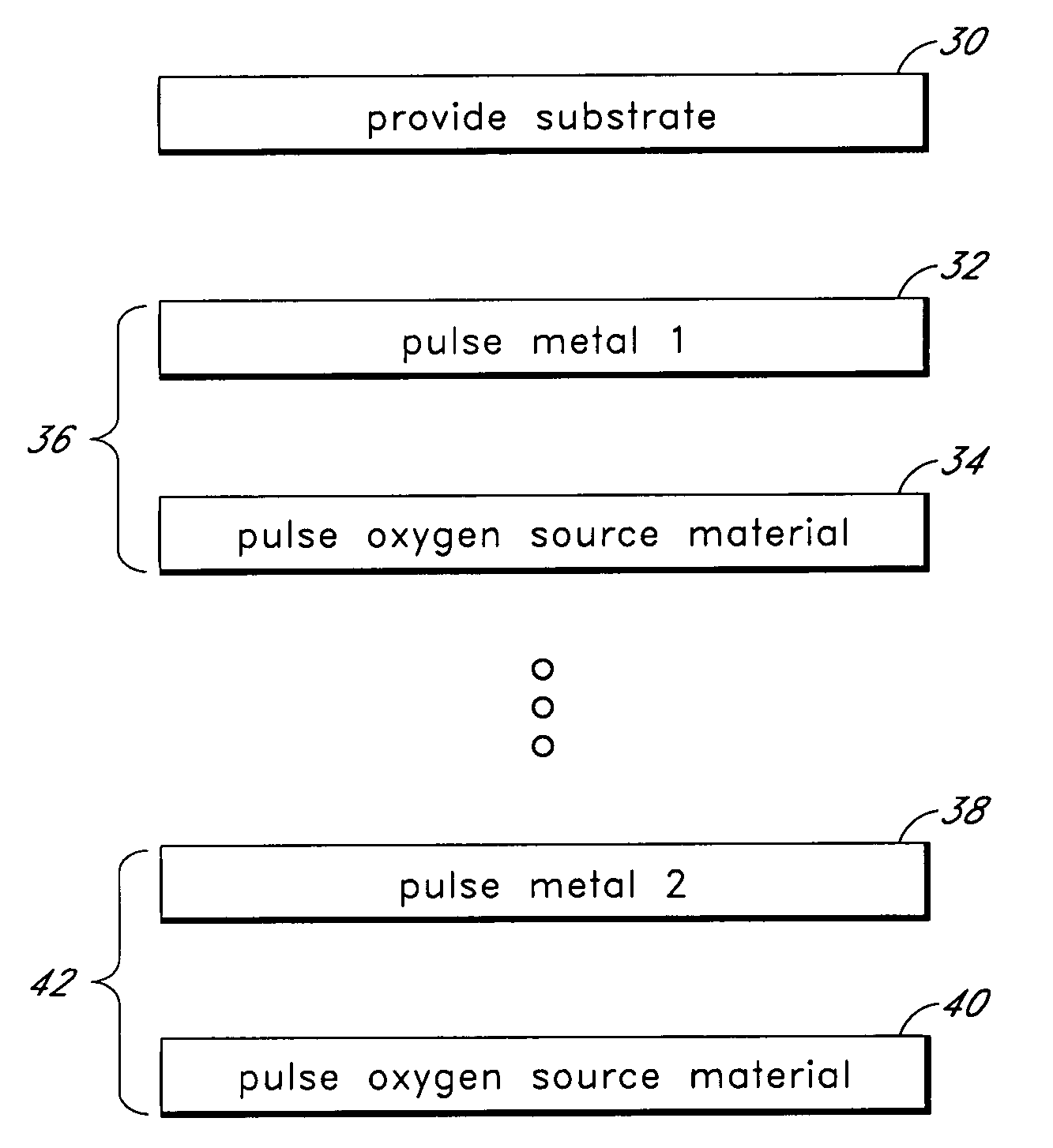
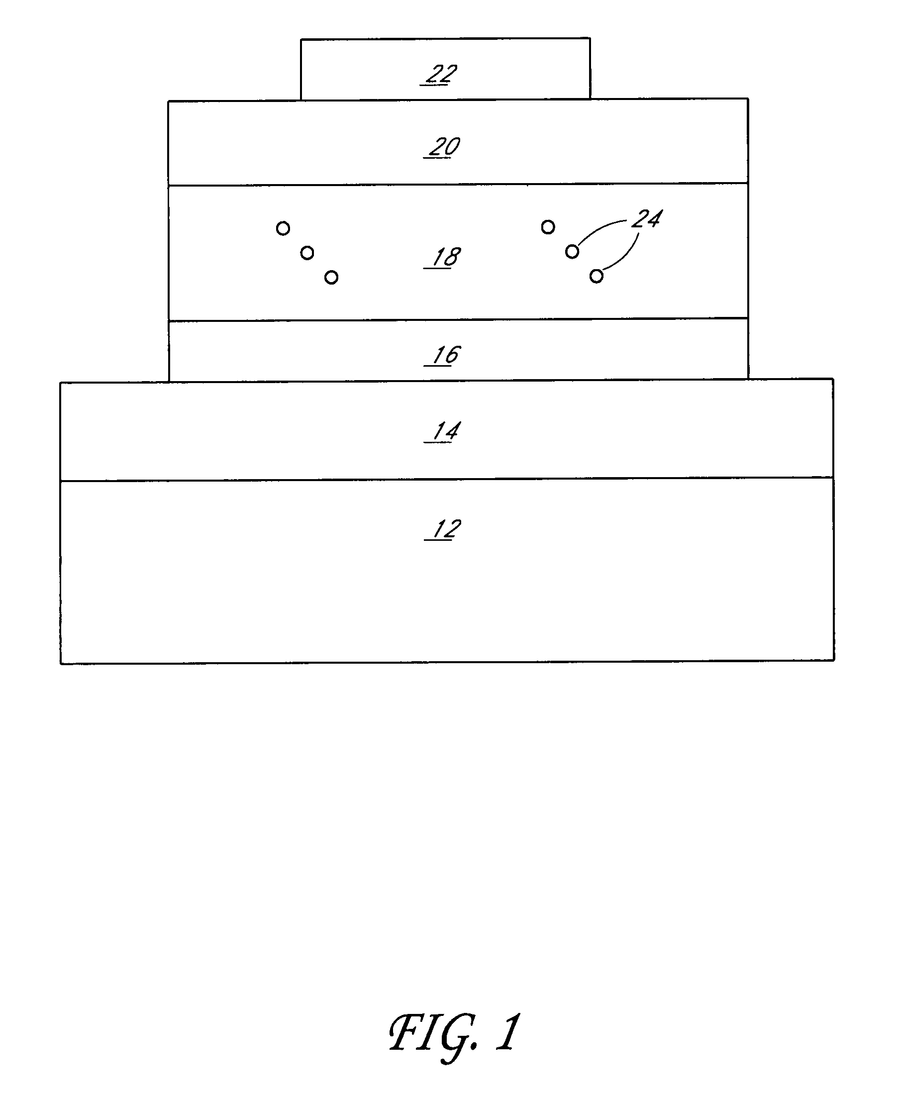
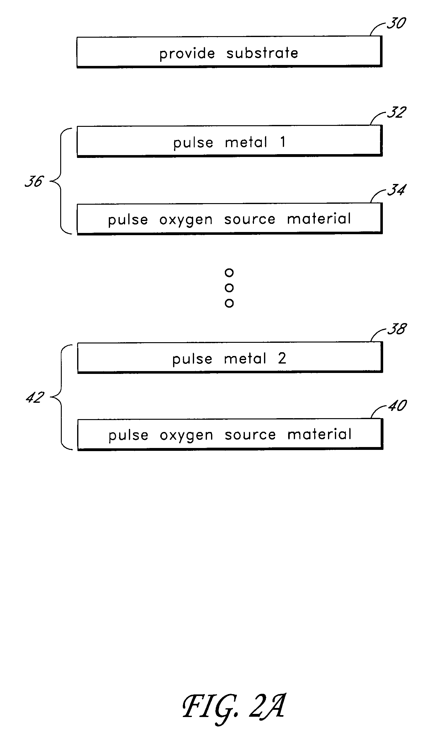
Method of forming complex oxide nanodots for a charge trap
a charge trapping and complex oxide technology, applied in the direction of basic electric elements, semiconductor devices, electrical equipment, etc., can solve the problems of charge retention failure in ono stacks thinner than 13.0 nm, scaling challenges for nonvolatile storage devices such as flash, rom, nrom,
- Summary
- Abstract
- Description
- Claims
- Application Information
AI Technical Summary
Problems solved by technology
Method used
Image

Examples
example
[0050]A silicon wafer was loaded into a vertical furnace for ALD processing from Tokyo Electron Ltd. of Japan. STO growth was carried out at temperatures in the range from 300 to 325° C. and pressure in the range of about 1-2 Torr. A first metal cycle included flushing the precursor line with THF, pulsing Ti(MPD)(thd)2 into the reactor for 60 seconds, flushing the precursor line with THF, evacuating the reactor, purging the substrate with Ar for 30 seconds, pulsing O3 into the reactor for 30 seconds, evacuating the reactor and subsequently purging the substrate with Ar for 20 seconds. A second metal cycle included flushing the precursor line with THF, pulsing Sr(THD)2 into the reactor for 30 seconds, flushing the precursor line with THF, reducing the pressure in the reactor to vacuum, purging the substrate with Ar for 30 seconds, pulsing O3 into the reactor for 30 seconds, reducing the pressure in the reactor to vacuum, and subsequently purging the substrate with Ar for 30 seconds. ...
PUM
| Property | Measurement | Unit |
|---|---|---|
| thick | aaaaa | aaaaa |
| thickness | aaaaa | aaaaa |
| diameter | aaaaa | aaaaa |
Abstract
Description
Claims
Application Information