

Semiconductor light emitting device
a technology of light-emitting devices and semiconductors, which is applied in the direction of semiconductor lasers, solid-state devices, lasers, etc., can solve problems such as light extracted from rough planes
- Summary
- Abstract
- Description
- Claims
- Application Information
AI Technical Summary
Problems solved by technology
Method used
Image

Examples
first embodiment
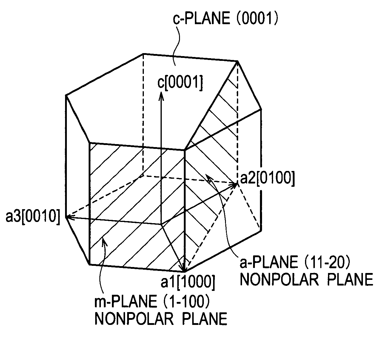
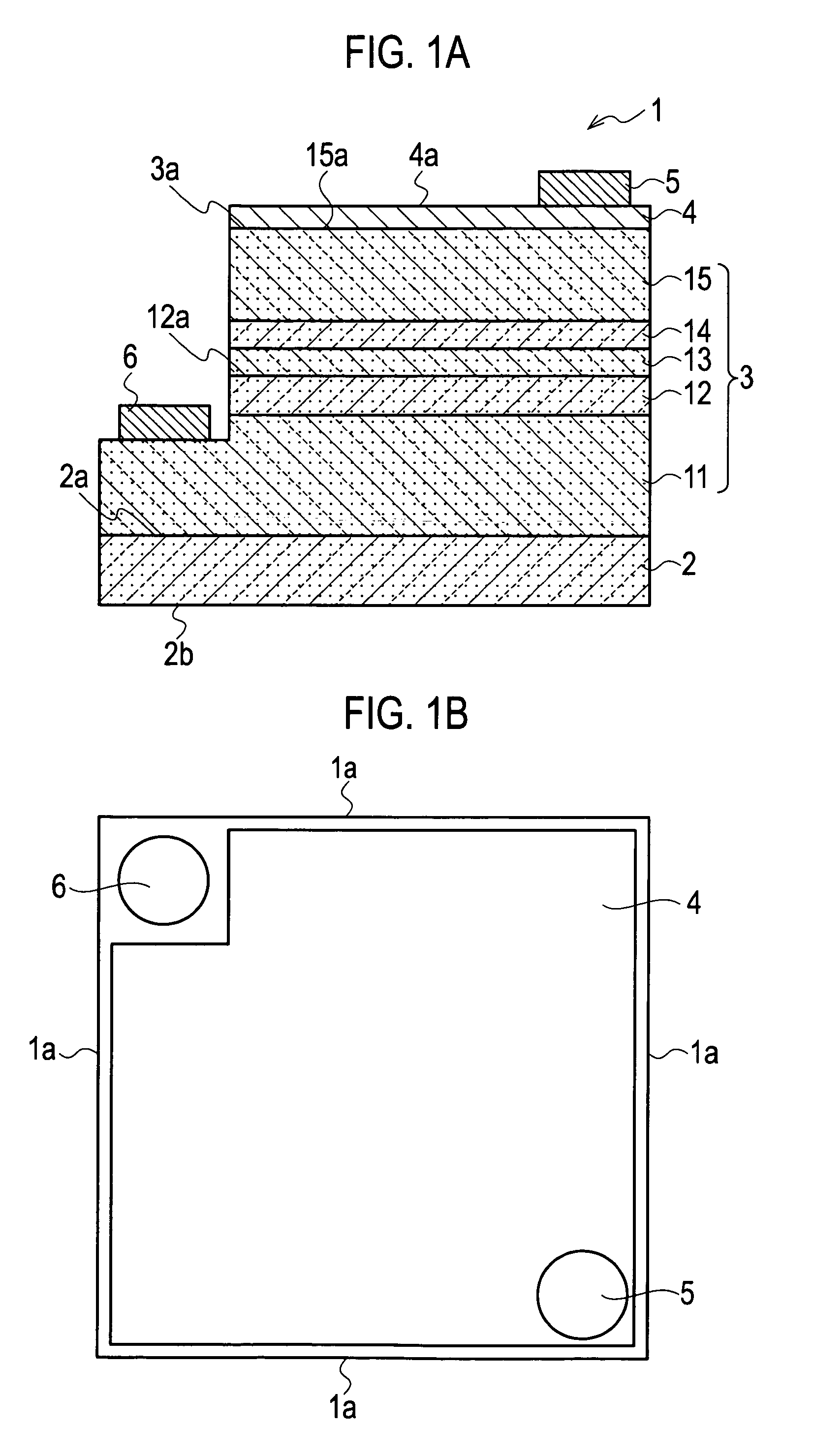
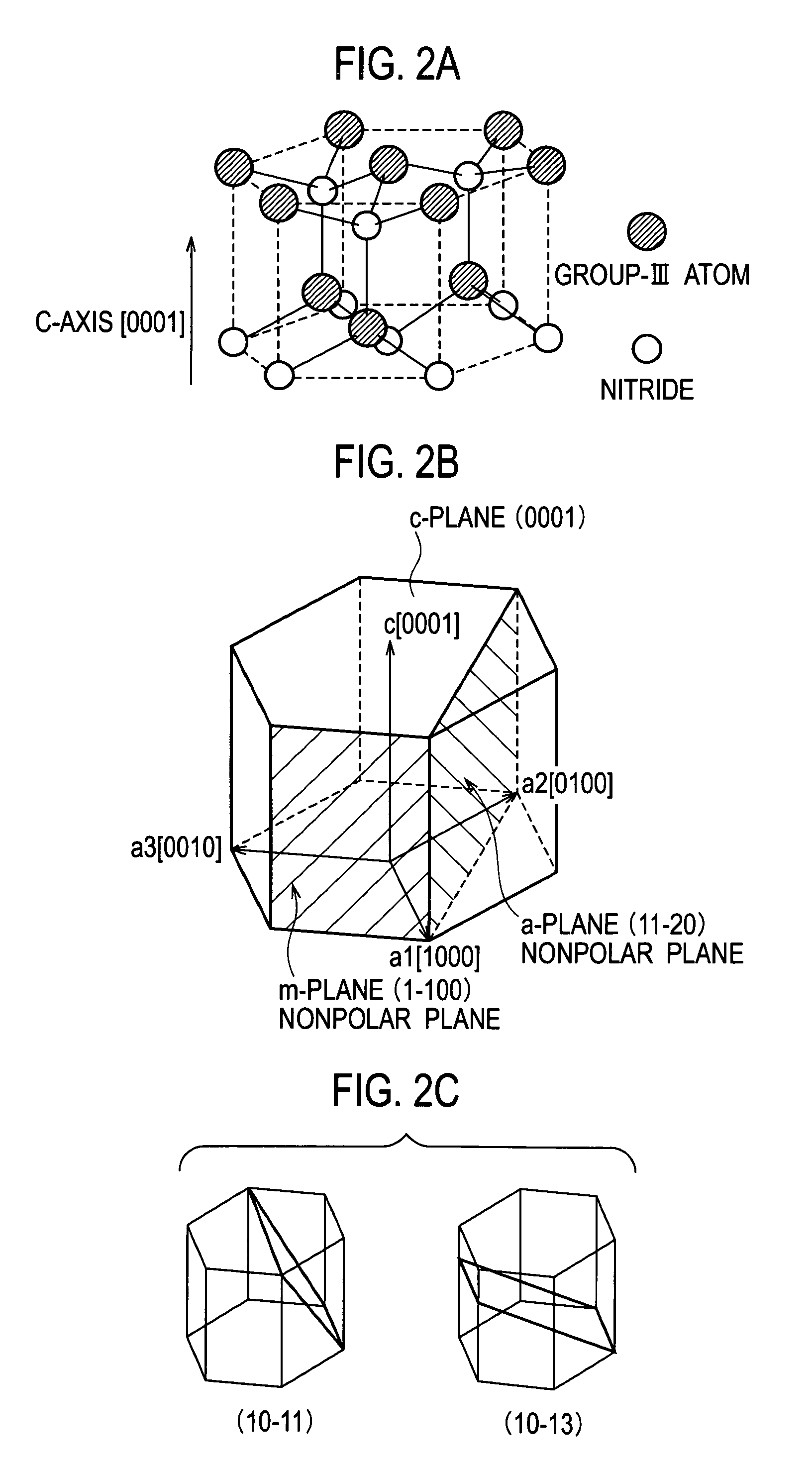
[0039]As shown in FIGS. 1A and 1B, a semiconductor light emitting device 1 according to a first embodiment of the present invention includes: a substrate 2; and a light emitting portion 3 disposed on a surface 2a of the substrate 2, in which side end surfaces 1a are specular surfaces. The side end surfaces 1a are composed of surfaces adjacent to the surface 2a of the substrate 2 and to a surface 3a as a growth principal surface of the light emitting portion 3. Here, “a specular surface” as each of the side end surfaces 1a refers to a surface in which a difference in irregularities of the side end surfaces 1a is equal to or less than a wavelength of a polarization generated by an active layer 12. The light emitting portion 3 includes an active layer 12 formed of a group III nitride semiconductor using a nonpolar plane or a semipolar plane as a growth principal surface 12a, and emits the polarization from the active layer 12. Moreover, as shown in FIGS. 1A and 1B, the semiconductor li...
second embodiment
[0078]A description will be made below of a manufacturing method of a semiconductor light emitting device 1 according to a second embodiment of the present invention. A configuration of the semiconductor light emitting device 1 manufactured by the manufacturing method according to the second embodiment is substantially similar to that of the semiconductor light emitting device 1 described in the first embodiment, and accordingly, a duplicate description will be omitted.
[0079]There is prepared such a substrate 2, which is formed of the single crystal of GaN, and in which the surface 2a is the m-plane, and the thickness is approximately 300 μm. The light emitting portion 3 is epitaxially grown on the surface 2a of the substrate 2 by the MOCVD method.
[0080]Next, by the sputtering method or the vacuum evaporation method, the first electrode portion 4 formed of ZnO is formed entirely on the light extraction surface 15a of the second semiconductor layer 15.
[0081]Subsequently, the first el...
third embodiment
[0086]A description will be made below of a manufacturing method of a semiconductor light emitting device 1 according to a third embodiment of the present invention. A configuration of the semiconductor light emitting device 1 manufactured by the manufacturing method according to the third embodiment is substantially similar to that of the semiconductor light emitting device 1 described in the first embodiment, and accordingly, a duplicate description will be omitted.
[0087]There is prepared such a substrate 2, which is formed of the single crystal of GaN, and in which the surface 2a is the m-plane, and the thickness is approximately 300 μm. The light emitting portion 3 is epitaxially grown on the surface 2a of the substrate 2 by the MOCVD method.
[0088]Next, by the sputtering method or the vacuum evaporation method, the first electrode portion 4 formed of ZnO is formed entirely on the light extraction surface 15a of the second semiconductor layer 15.
[0089]The first electrode portion ...
PUM
 Abstract
Description
Claims
Application Information