Semiconductor light emitting device and fabrication method thereof

a technology of semiconductor light emitting device and fabrication method, which is applied in the manufacture of semiconductor/solid-state devices, semiconductor devices, and devices containing threading dislocations upwardly, and achieves excellent luminous efficiency

Inactive Publication Date: 2005-11-22
SAMSUNG ELECTRONICS CO LTD
View PDF21 Cites 417 Cited by
  • Summary
  • Abstract
  • Description
  • Claims
  • Application Information

AI Technical Summary

Benefits of technology

[0016]An object of the present invention is to provide a semiconductor light emitting device excellent in luminous efficiency even if the device ha

Problems solved by technology

The technique of forming a nitride semiconductor such as a gallium nitride based compound semiconductor by vapor-phase growth has an inconvenience that neither a substrate being lattice matching with the nitride semiconductor nor a substrate with a low dislocation density is present.
The above-described light emitting diode formed by selective growth, however, has a problem that the diode contains threading dislocations upwardly extending from the substrate.
Another problem is that since the apex and/or the upper surface is surrounded by a side plane composed of a facet where the growth rate is low, the supply of a source gas becomes too large, tending to degrade the crystallinity of the apex and/or the upper surface.
As a further problem, if the area of the apex and/or the upper surface is smaller than that of the substrate, it is difficult to control the film thickness and the composition of a mixed crystal at the apex and/or the upper surface.
Accordingly, even if a semiconductor device having a three-dimensional structure is formed by selective growth, the crystallinity of the

Method used


Image

  • Semiconductor light emitting device and fabrication method thereof
  • Semiconductor light emitting device and fabrication method thereof
  • Semiconductor light emitting device and fabrication method thereof

Examples


Embodiment Construction

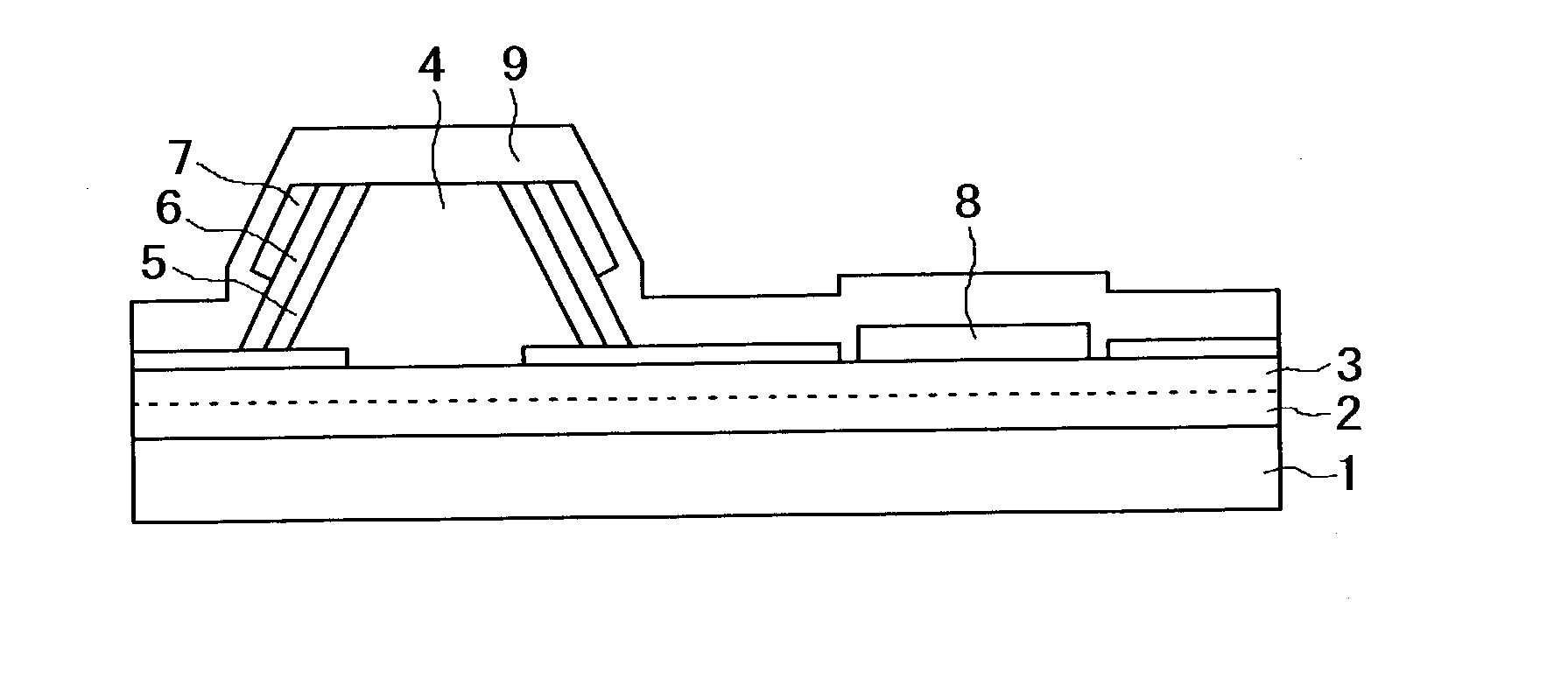
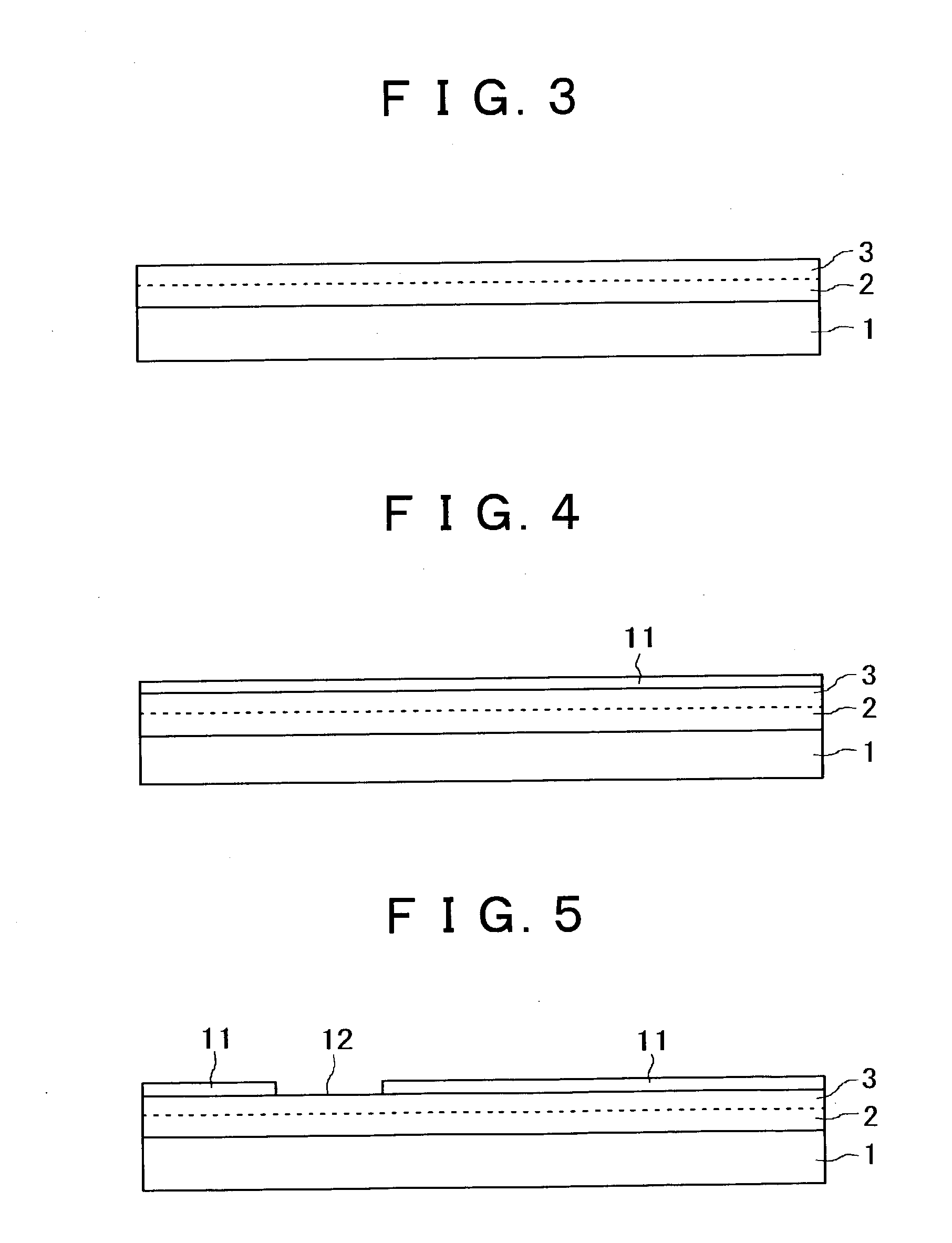
[0079]Hereinafter, the present invention will be described in detail with reference to the drawings. It is to be noted that in the drawings, parts of a semiconductor light emitting device of the present invention are sometimes depicted on a scale different from the actual scale for the sake of convenience of description.

[0080]A semiconductor light emitting device of the present invention is characterized by including a crystal layer formed on a substrate, the crystal layer having a tilt crystal plane tilted from the principal plane of the substrate, and a first conductive type layer, an active layer, and a second conductive type layer, which are formed on the crystal layer in such a manner as to extend within planes parallel to the tilt crystal plane, wherein the device has a shape formed by removing the apex and its vicinity of the stacked layer structure formed on the substrate.

[0081]The substrate used herein is not particularly limited insofar as it allows a crystal layer having ...


PUM


Abstract

A semiconductor light emitting device includes a crystal layer formed on a substrate, the crystal layer having a tilt crystal plane tilted from the principal plane of the substrate, and a first conductive type layer, an active layer, and a second conductive type layer, which are formed on the crystal layer in such a manner as to extend within planes parallel to the tilt crystal plane, wherein the device has a shape formed by removing the apex and its vicinity of the stacked layer structure formed on the substrate. Such a semiconductor light emitting device is excellent in luminous efficiency even if the device has a three-dimensional device structure. The present invention also provides a method of fabricating the above semiconductor light emitting device.

Description

[0001]This application claims priority to Japanese Patent Application Number JP2002-010685 filed Jan. 18, 2002, which is incorporated herein by reference.BACKGROUND OF THE INVENTION[0002]The present invention relates to a semiconductor light emitting device and a fabrication method thereof.[0003]Nitride based III–V compound semiconductors such as GaN, AlGaN and InGaN have forbidden band widths ranging from 1.8 eV to 6.2 eV, and therefore, they are theoretically capable of realizing light emitting devices allowing emission of light having wavelengths in a wide range from a long-wavelength side (for example, red) to a short-wavelength side (for example, ultraviolet). From this viewpoint, in recent years, such nitride based III–V compound semiconductors have become a focus of attention as materials for light emitting devices.[0004]In the case of fabricating a light emitting diode (LED) or a semiconductor laser by using nitride based III–V compound semiconductors, it is required to stac...

Claims


Application Information

Patent Timeline
IPC IPC(8): H01L33/00H01L33/16H01L33/24H01L33/28H01L33/32H01L33/38H01L33/06
CPCH01L33/18H01L33/24
Inventor SUZUKI, JUNOKUYAMA, HIROYUKIBIWA, GOSHIMORITA, ETSUO
Owner SAMSUNG ELECTRONICS CO LTD
Why Eureka
Try Eureka