

Low temperature thin film transistor process, device property, and device stability improvement
a thin film transistor, low temperature technology, applied in the direction of transistors, semiconductor devices, electrical equipment, etc., can solve problems such as transistor failur
- Summary
- Abstract
- Description
- Claims
- Application Information
AI Technical Summary
Benefits of technology
Problems solved by technology
Method used
Image

Examples
examples
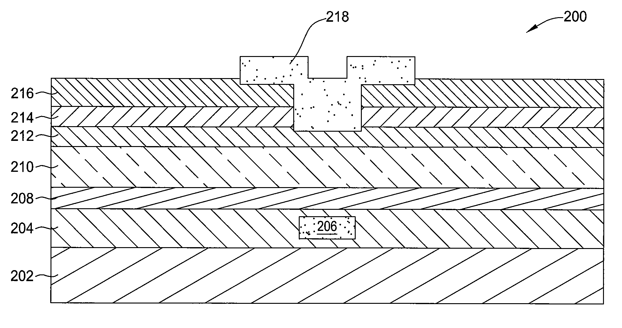
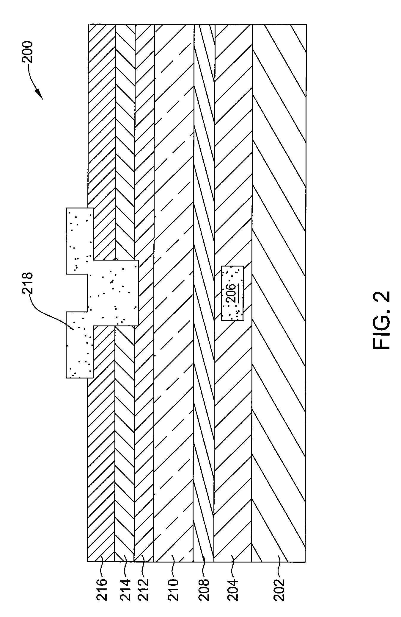
[0057]In a first example, a TFT was formed by depositing a silicon rich silicon nitride layer over a substrate having a bottom gate layer formed thereon. The silicon rich silicon nitride layer was deposited to a thickness of about 2800 Å. A silicon nitride layer was formed in the same process chamber over the silicon rich silicon nitride layer to a depth of about 500 Å. A first amorphous silicon layer was formed to a thickness of about 300 Å over the silicon nitride layer. A second active layer of amorphous silicon was then deposited at a high deposition rate over the first active layer to a thickness of about 1600 Å in the same process chamber. A doped amorphous silicon layer about 400 Å thick was deposited over that, again in the same chamber. Metal contacts and passivation layer were added on top. Process conditions for the various deposition steps are given below in Table 1.
TABLE 1Process Conditions for Example 1SiH4NH3N2H2PH3Dep.RateRateRateRateRatePowerPressureSpacingTemp.Rate...
PUM
 Abstract
Description
Claims
Application Information