Semiconductor substrate

a technology of semiconductors and substrates, applied in the field of semiconductor substrates, can solve the problems of excessive etching of intersecting portions of v-grooves, affecting the quality of separation, and destroying structures, so as to improve process takt and reduce separation quality

Active Publication Date: 2010-12-28
TDK CORPARATION
View PDF10 Cites 123 Cited by
  • Summary
  • Abstract
  • Description
  • Claims
  • Application Information

AI Technical Summary

Benefits of technology

[0010]The present invention is made in consideration of the disadvantages described above, and an object thereof is to improve process takt without decreasing separation quality when separating a semiconductor substrate on which a plurality of semiconductor elements are formed into individual semiconductor elements and forming individual semiconductor devices.
[0013]As described above, since grooves are formed with the exception of intersections of the separating lines or, in other words, since groove intersections where it is extremely difficult to control etching have been removed, the formation of grooves can be performed in an extremely easy and stable manner. In addition, since a structure is achieved in which the substrate is thin at the groove portions and stress can be more readily concentrated during separation using cleavages or the like, separation can now be performed with good rectilinearity and in a stable manner.

Problems solved by technology

However, since diaphragm structures and beam structures are structurally fragile, there is a risk that the pressure generated by the water may destroy the structures.
However, with this method, if the semiconductor substrate 101 is thick, splitting cannot be achieved depending on the modified region 109 produced by a single scan.
However, with this method, since the erosion due to anisotropic etching of portions at which the longitudinal and lateral V-grooves intersect differs from the erosion of other portions, excessive etching may prevent etching from stopping at the (111)-oriented surface and etching may proceed to a (211)-oriented surface.
For example, when concurrently forming V-grooves in a process of forming a diaphragm structure requiring deeper etching than that required for V-grooves, intersecting portions of the V-grooves end up being excessively etched, sometimes to the extent of penetrating the semiconductor substrate.
Consequently, the strength of the semiconductor substrate deteriorates significantly, causing the semiconductor substrate to break during handling.
However, in the case as described above where only grooves on separating lines in either the longitudinal direction or the lateral direction are formed as continuous grooves, since the continuous grooves are not uniformly disposed with respect to the four sides of individual semiconductor devices to be separated, stress tends to concentrate on sides on which the continuous grooves are formed and damage originating at such sides may occur in the semiconductor device.
The formation of continuous grooves causes deterioration in strength and may lead to damage to the semiconductor substrate during handling.
However, in this case, since the grooves are not continuous, the rectilinearity of separation decreases, resulting in nonuniform shapes of semiconductor devices after separation and, in particular, inhomogeneous dimensions of the respective sides.
As a result, for example, the pick-up rate of collets picked up at the sides of semiconductor devices in a subsequent process declines, resulting in lower productivity.

Method used


Image

  • Semiconductor substrate
  • Semiconductor substrate
  • Semiconductor substrate

Examples


Embodiment Construction

[0037]An embodiment of the present invention will now be described with reference to the drawings.

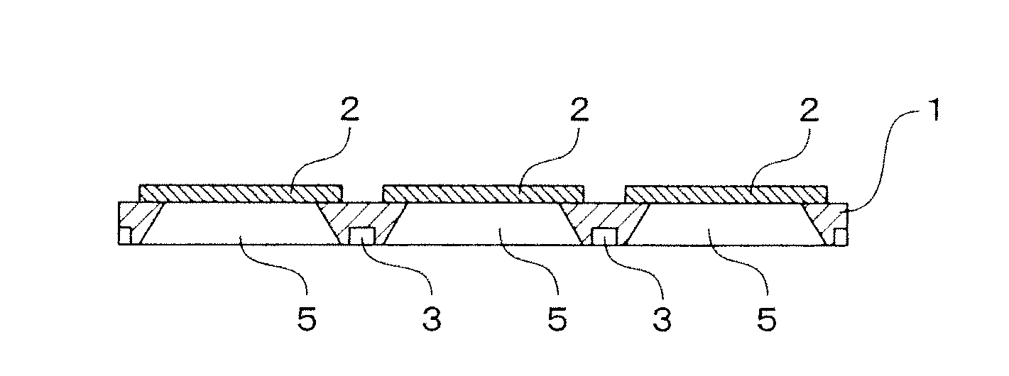
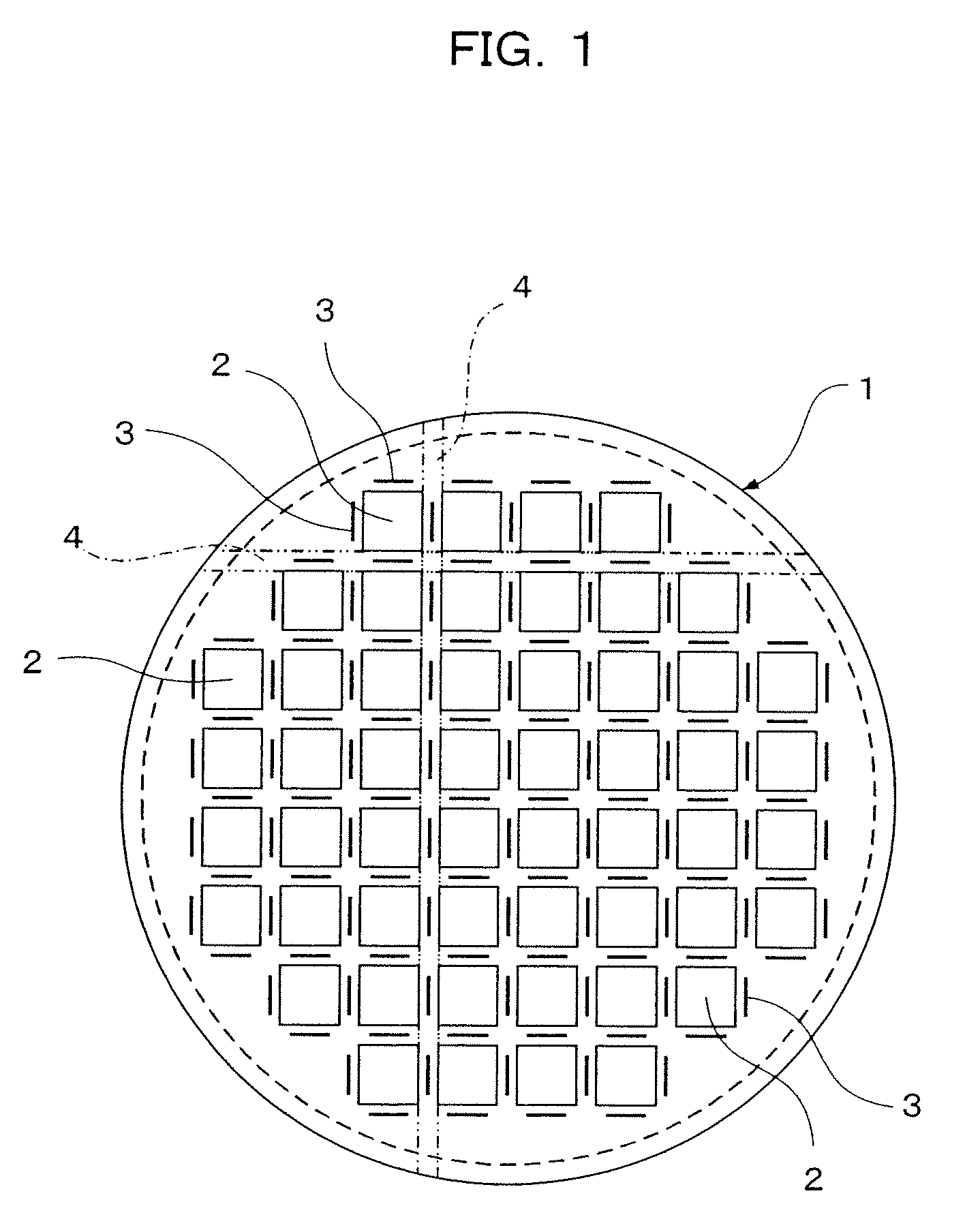
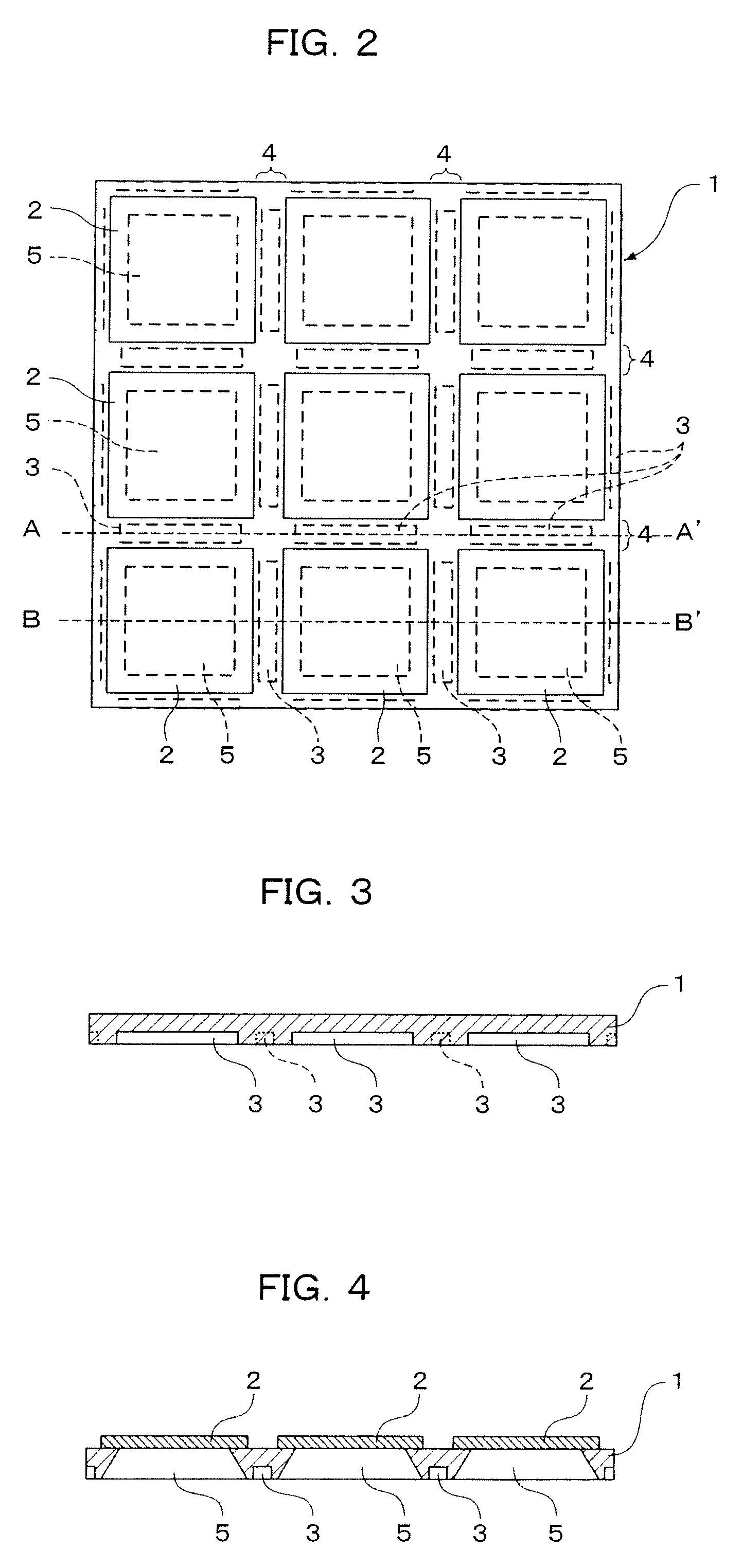
[0038]In FIGS. 1 to 4, a semiconductor substrate 1 is made up of Si monocrystals, and a plurality of semiconductor elements 2 in which functional elements are constructed are formed in a grid pattern on one of the faces of the semiconductor substrate 1. The portions of the semiconductor elements 2 become diaphragm pressure sensors (semiconductor devices) after separation. As such, the semiconductor elements 2 themselves are made thin so as to become sensing sections, while depressions 5 are formed on rear face-sides of the semiconductor elements 2, constituting diaphragm structures. An example of such a diaphragm pressure sensor is a microphone sensor, in which air vibrated by sound vibrates a diaphragm, and the displacement of the diaphragm varies the capacity of a conductor between a receiving-side diaphragm and a vibrating-side diaphragm to convert the sound into a vibrational freque...


PUM

PropertyMeasurementUnit
inclination angleaaaaaaaaaa
thicknessaaaaaaaaaa
thicknessaaaaaaaaaa

Abstract

A semiconductor substrate (1) includes a plurality of semiconductor elements (2) in which functional elements are constructed and which is formed in a grid pattern, wherein continuous linear grooves (3) are formed on longitudinal and lateral separating lines (4) that individually separate the plurality of semiconductor elements (2) with the exception of intersections of the separating lines (4) and portions corresponding to corners of each semiconductor element (2).

Description

FIELD OF THE INVENTION[0001]The present invention relates to a semiconductor substrate, a semiconductor device, and a method of manufacturing the same.BACKGROUND OF THE INVENTION[0002]Semiconductor devices having partially-thinned structures as typified by MEMS (microelectromechanical system) include MEMS pressure sensors and MEMS accelerometers. Generally, a plurality of such sensors is concurrently formed in a semiconductor wafer process so as to acquire a diaphragm structure or a beam structure, and is subsequently individually separated. As for the separation, the most common method involves rotating a circular dicing saw to which diamond or c-BN particles are secured at high speed to perform a fracturing process. The process is performed while running water for removing fractured waste and suppressing frictional heat. However, since diaphragm structures and beam structures are structurally fragile, there is a risk that the pressure generated by the water may destroy the structu...

Claims


Application Information

Patent Timeline
Patent Type & Authority Patents(United States)
IPC IPC(8): H01L23/544
CPCB23K26/0057B23K26/4075B23K26/421B28D5/0011H01L2924/10158H01L2924/16195H01L2924/16235B23K26/60B23K26/40B23K26/53B23K2103/50B81C1/00888
Inventor UTSUMI, MASAKIKUMAKAWA, TAKAHIRO
Owner TDK CORPARATION
Why Eureka
Try Eureka