Conductive contact unit and conductive contact

Inactive Publication Date: 2011-01-11
NHK SPRING CO LTD
View PDF13 Cites 6 Cited by
  • Summary
  • Abstract
  • Description
  • Claims
  • Application Information

AI Technical Summary

Benefits of technology

[0010]The present invention is invented in consideration of the above. An object of the present invention is to provide a conductive contact unit and a conductive contact that can support the smaller arrangement intervals, that enables the operator to look at the contact of the test object easily from the top, and that can achieve a stable electrical contact without applying the excessive load.
[0016]According to the present invention, provided with are a conductive contact holder including a plurality of first guiding grooves and a plurality of the second guiding grooves facing the first guiding grooves, the first guiding grooves being engaged with one longitudinal outside ends of the conductive contacts to hold the conductive contacts in a slidable manner, respectively, and the second guiding grooves being engaged with outside ends other than the outside ends of the conductive contacts engaged with the first guiding grooves to hold the conductive contacts in a slidable manner, respectively; a plurality of such plate-like conductive contacts, each of which including a first contacting element that is brought in physical contact with one of the different circuitries, a second contacting element that is brought into physical contact with one of the different circuitries other than that brought into contact with the first contacting element, an elastic element that is interposed between the first contacting element and the second contacting element and is extensible in a longitudinal direction thereof, a first connecting element that connects the elastic element and the first contacting element, and a second connecting element that connects the elastic element and the second contacting element, that has an opening penetrating therethrough in a thickness direction, and that projects from ends of the second guiding grooves toward outside of the conductive contact holder when being held inside the conductive contact holder; and a bar-shaped member that penetrates through the openings formed on the respective second connecting elements of the conductive contacts, and is fixed onto the conductive contact holder. In this manner, the narrower arrangement intervals can be supported, and the contact with the test object can be visually checked from the top easily. Moreover, a stable electrical contact can be achieved without applying an excessive load.
[0017]According to the present invention, provided are a first contacting element that is brought into physical contact with one of the different circuitries; a second contacting element that is brought into physical contact with one of the different circuitries other than that brought into contact with the first contacting element; an elastic element that is interposed between the first contacting element and the second contacting element, and is extensible in a longitudinal direction; a first connecting element that connects the elastic element and the first contacting element; and a second connecting element that connects the elastic element and the second contacting element and has an opening penetrating therethrough in a thickness direction, and the second contacting element projects from a width-direction outside end of the second connecting element in the width direction. In this manner, the smaller arrangement intervals can be supported, and the contact with the test object can be visually checked from the top easily, when the conductive contact is held in the conductive contact holder. Moreover, a stable electrical contact can be achieved without applying an excessive load.

Problems solved by technology

However, minimum possible intervals thereof are limited by several conditions, such as physical strength of the conductive contact holder on which these guiding holes are formed.
Therefore, even though the conductive contacts themselves have a structure suitable for smaller arrangement intervals, not sufficient devices have been suggested for the structure of the conductive contact holder.
Therefore, considering the conductive contact unit as a whole, it has been sometimes difficult to reduce the arrangement intervals of the conductive contacts.
This leads to an increased physical burden to the operator when the greater number of times the test is performed.
Therefore, it has been impossible to sufficiently remove an oxidized film formed on the surface of the test object, or dust attached thereon.
Therefore, it has been sometimes impossible to obtain a stable electric contact.
In such a situation, an excessive load could be applied onto the conductive contacts.

Method used


Image

  • Conductive contact unit and conductive contact
  • Conductive contact unit and conductive contact
  • Conductive contact unit and conductive contact

Examples


first embodiment

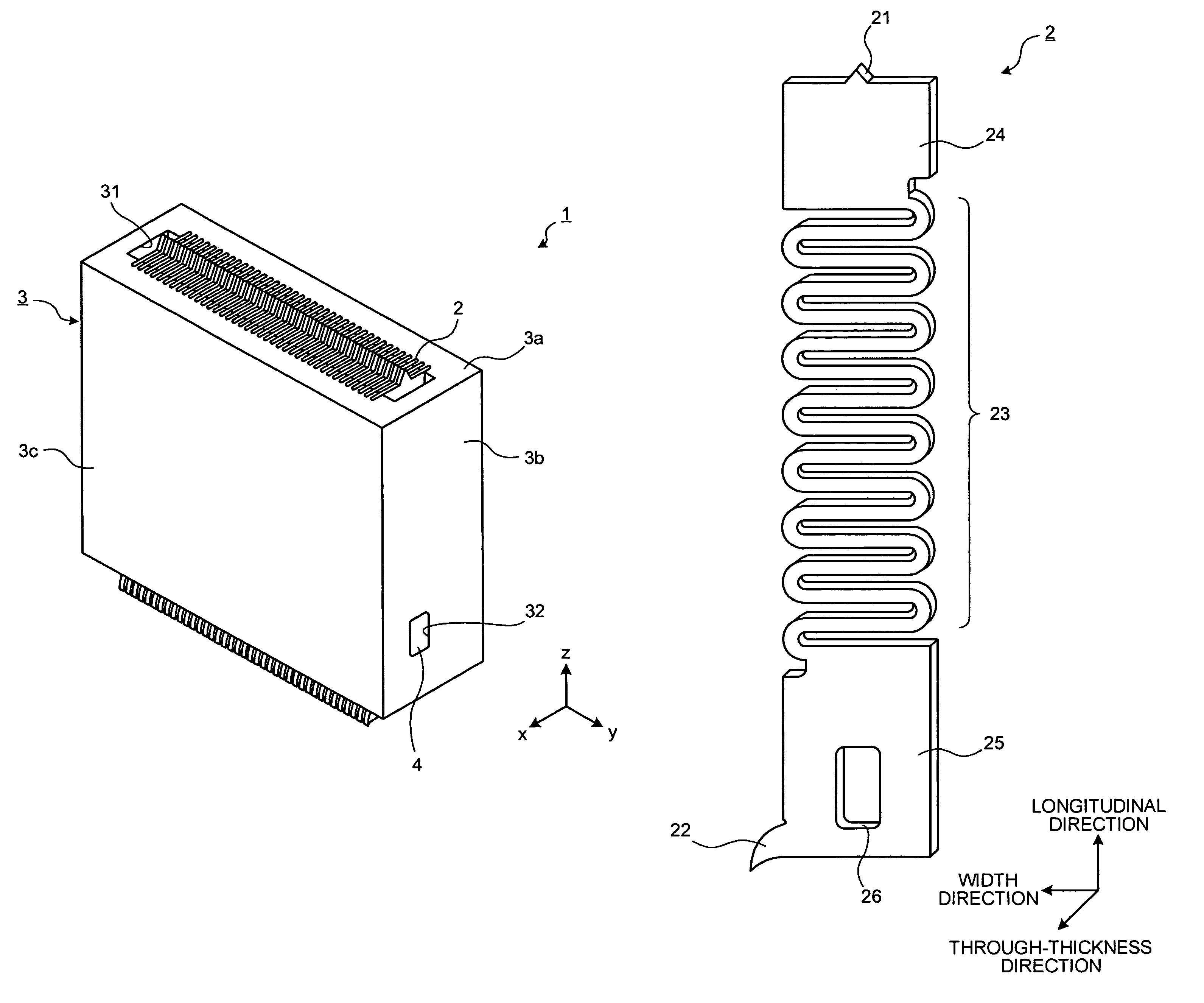
[0053]FIG. 1 is a perspective view of a structure of a conductive contact unit according to a first embodiment of the present invention. A conductive contact unit 1, shown in FIG. 1, is used for testing the conductive state or operating characteristics of testing a circuitry, such as a liquid crystal panel that is a test object. The conductive contact unit 1 includes a plurality of conductive contacts 2, a conductive contact holder 3 that contains the conductive contacts 2, and a bar-shaped member 4 that is fastened to the conductive contact holder 3 and supports the conductive contacts 2.

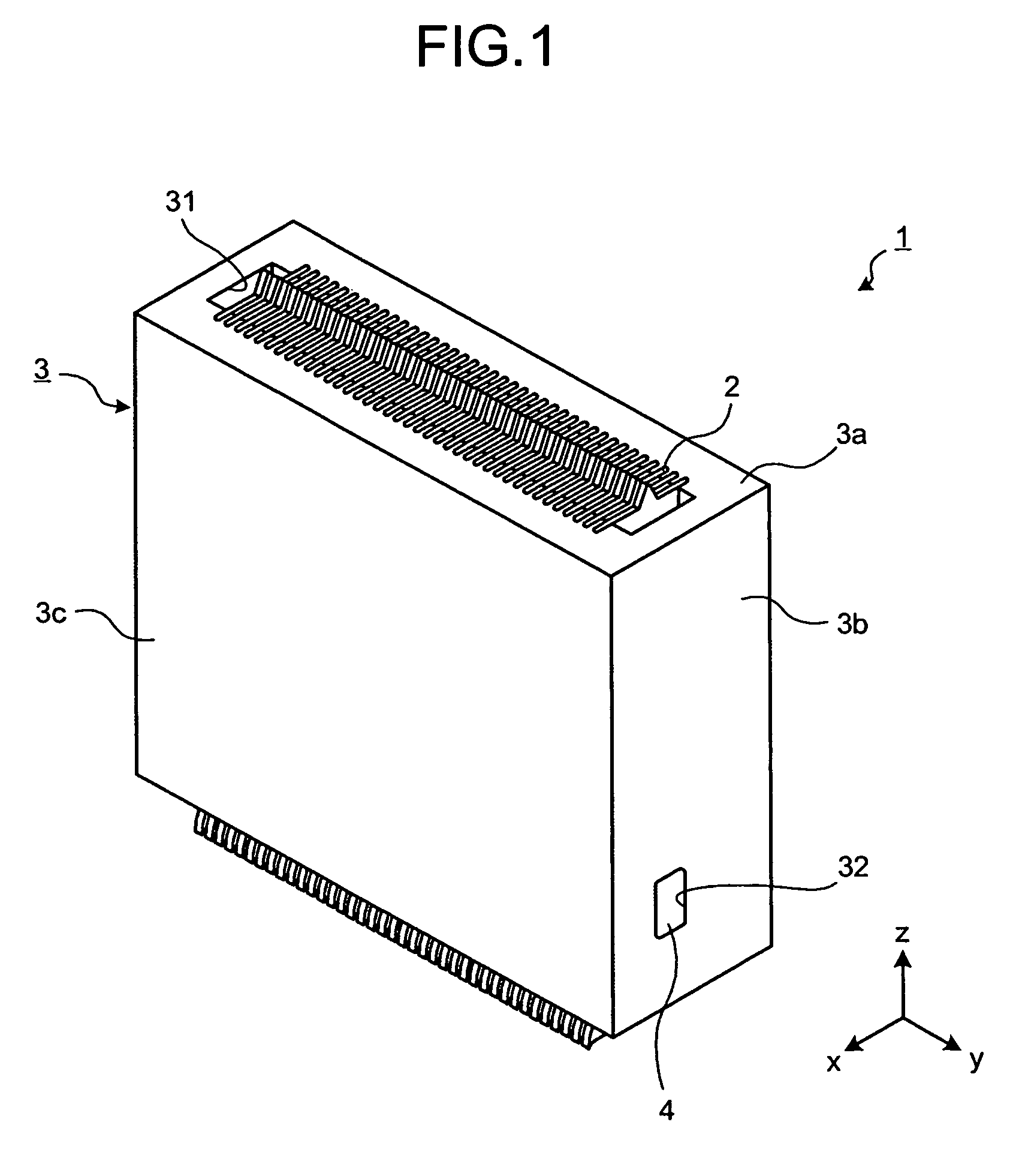
[0054]The conductive contact 2 will be now explained in detail. FIG. 2 is a diagram of a structure of the conductive contact 2 according to the first embodiment. In the following description, the vertical direction in FIG. 2 will be referred to as a “longitudinal direction of the conductive contact 2”, the horizontal direction in FIG. 2 will be referred to as a “width direction of the conductive co...

second embodiment

[0082]FIG. 7 is a diagram of a structure of a conductive contact according to a second embodiment of the present invention. In the following description, the vertical direction in FIG. 7 will be referred to as a “longitudinal direction of a conductive contact 5”, the horizontal direction in FIG. 7 will be referred to as a “width direction of the conductive contact 5”, and the direction intersecting with the longitudinal direction and the width direction will be referred to as a “through-thickness (thickness) direction of the conductive contact 5”, respectively.

[0083]The conductive contact 5 shown in FIG. 7 is provided to establish an electrical connection between different circuitries. The conductive contact 5 includes: a first contacting element 51 that is brought into physical contact with a predetermined circuitry (specifically, a circuitry including a test circuit); a second contacting element 52 that is brought into physical contact with a circuitry other than that brought into...


PUM


Abstract

A conductive contact unit includes plate-like conductive contacts for electrically connecting different circuitries. Each conductive contact includes a first contacting element to be brought in physical contact with one circuitry, a second contacting element to be brought in physical contact with another circuitry, an elastic element, between the first contacting element and the second contacting element, a first connecting element that connects the elastic element and the first contacting element, and a second connecting element that connects the elastic element and the second contacting element and that has an opening. The conductive contact unit also includes a conductive contact holder including first guiding grooves and second guiding grooves facing the first guiding grooves. The conductive contact holder holds the conductive contacts with both longitudinal outside ends of each conductive contact being slidably engaged with the first and the second guiding grooves.

Description

BACKGROUND OF THE INVENTION[0001]1. Field of the Invention[0002]The present invention relates to a conductive contact unit and a conductive contact that are brought into contact with an electrode or a terminal that transmits and receives an electrical signal upon testing a conductive state or testing operating characteristics of an electronic component such as a liquid crystal panel or a semiconductor integrated circuit.[0003]2. Description of Related Art[0004]In a technological field of electrical characteristic testing of a test object such as a semiconductor integrated circuit, there is a known technology related to a conductive contact unit. The conductive contact unit includes a plurality of conductive contacts, each of which is arranged correspondingly to a connecting terminal of the semiconductor integrated circuit, and provides electrical conductivity by bringing the conductive contacts into physical contact with the connecting terminals. A structure of the conductive contac...

Claims


Application Information

Patent Timeline
IPC IPC(8): H01R12/00
CPCG01R1/06722G01R1/06738G01R1/07307G01R1/067
Inventor RIKIMARU, TAIICHIISHIKAWA, KOJITOMINAGA, JUN
Owner NHK SPRING CO LTD
Why Eureka
Try Eureka