Electronic device and electronic apparatus

a technology of electronic devices and electronic components, applied in the field of electronic devices, can solve the problems of deterioration of the electrical contact state and to conductive disconnection, the possibility of conductive disconnection between the ic chip b>1021/b> and the glass substrate b>1011/b>, and the difficulty of obtaining a predetermined amount of elastic deformation of the conductive particles, so as to prevent deterioration of a good electrical contact state, the effect o

Inactive Publication Date: 2010-07-08
SEIKO EPSON CORP
View PDF7 Cites 2 Cited by
  • Summary
  • Abstract
  • Description
  • Claims
  • Application Information

AI Technical Summary

Benefits of technology

[0012]An advantage of the invention is to provide an electronic device that withstand temperature changes and maintain stable electric contact.
[0013]According to an aspect of the invention, an electronic device includes: a semiconductor device including a semiconductor chip having an electrode; a convex-shaped resin protrusion provided on a surface of the semiconductor chip, the surface having the electrode; and wiring having a plurality of electrical coupling sections which are aligned on the resin protrusion and electrically coupled to the electrode, and a wiring substrate containing a wiring pattern, in that: the semiconductor device is mounted to the wiring substrate so that the electrical coupling sections and the wiring pattern are brought into contact and electrically coupled with each other, and the plurality of electrical coupling sections brought into contact with the wiring pattern include curved or bent shapes projecting in a longitudinal direction of the resin protrusion.
[0014]In this case, the plurality of electrical coupling sections brought into contact with the wiring pattern include curved or bent shapes that project in the longitudinal direction of the resin protrusion. Because of these curved or bent shapes, the length of sides constituting each of the plurality of electric coupling sections that have been brought into contact with the wiring pattern may increase. This may increase an electrical contact area, as compared to a straight-lined shape that is not curved or bent. Therefore, despite the variation in the thermal expansion of the wiring substrate, resin protrusion, and the like that constitute the electronic device, the electrical coupling sections may maintain and prevent deterioration of a good electrical contact state. It is therefore possible to provide an electronic device that can withstand temperature changes and maintain stable electric contact.
[0015]It is preferable that, in the electronic device, the plurality of electrical coupling sections brought into contact with the wiring pattern be provided such that a first length from an end thereof in a width direction of the resin protrusion to a hypothetical center line of the resin protrusion in the longitudinal direction is longer than a second length from a center thereof in the width direction of the resin protrusion to the hypothetical center line.
[0016]It is preferable that, in the electronic device, the plurality of electrical coupling sections in contact with the wiring pattern be provided such that the first length from the end thereof in the width direction of the resin protrusion to the hypothetical center line of the resin protrusion in the longitudinal direction is shorter than the second length from the center thereof in the width direction of the resin protrusion to the hypothetical center line.
[0017]In these cases, the plurality of electrical coupling sections brought into contact with the wiring pattern are provided such that the length from its end in the width direction of the resin protrusion to the hypothetical center line of the resin protrusion in the longitudinal direction is longer or shorter than (is different from) the length from its center in the width direction of the resin protrusion to the hypothetical center line. Thus, the plurality of electrical coupling sections brought into contact with the wiring pattern have shapes projecting in the longitudinal direction of the resin protrusion. Because of this projection, the length of sides constituting each of the plurality of electric coupling sections that have been brought into contact with the wiring pattern increases. This may increase the electrical contact area, as compared to the straight-lined shape with no such projection. As a result, despite the variation in the thermal expansion of the wiring substrate, resin protrusion, and the like that constitute the electronic device, the electrical coupling sections may maintain and prevent deterioration of a good electrical contact state. It is therefore possible to provide the electronic device that can withstand temperature changes and maintain the stable electric contact.

Problems solved by technology

However, it is extremely difficult to obtain a predetermined amount of elastic deformation of the conductive particles 1222a because of their minuteness.
With the increase in the deformation amount of the resin protrusion 1012, the variation in the deformation amount of each constituent increases, thereby possibly leading to deterioration of the electrical contact state and to conductive disconnection.
In this case, the possibility of conductive disconnection between the IC chip 1021 and the glass substrate 1011 is a problem.

Method used


Image

  • Electronic device and electronic apparatus
  • Electronic device and electronic apparatus
  • Electronic device and electronic apparatus

Examples


Embodiment Construction

[0037]Embodiments of the invention will now be described with reference to the drawings, using an electrooptical device as an example of the electronic device.

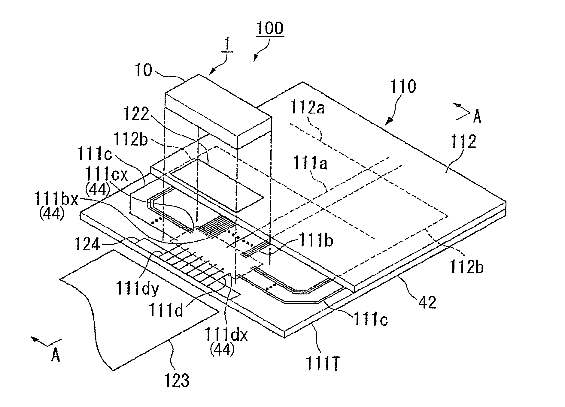
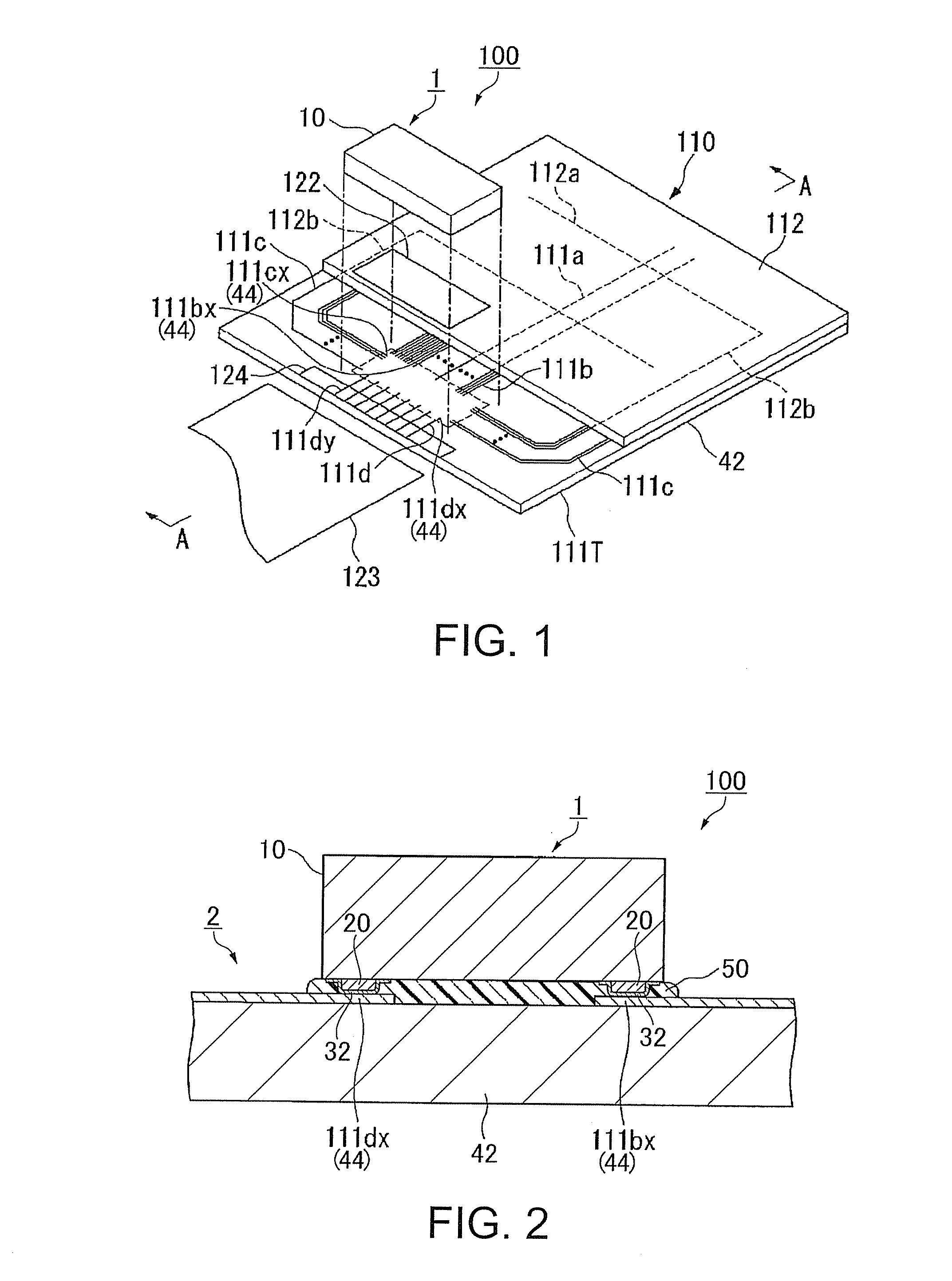
[0038]FIG. 1 is a pattern diagram showing a liquid crystal device which is one embodiment of the electrooptical device. A liquid crystal display 100 shown in the drawing includes: a liquid crystal panel 110; and a semiconductor device 1 containing a semiconductor chip 10 for driving liquid crystal 10 (hereunder referred to as semiconductor chip 10). If necessary, incidental members such as a polarizing plate, a reflecting sheet, and a backlight (not shown) may be provided.

[0039]Structure of Electrooptical Device

[0040]The liquid crystal panel 110 as a wiring substrate includes a base substrate 42 and a substrate 112 made of e.g. glass or plastic. The base substrate 42 and the substrate 112 are arranged opposite from each other and attached to each other with e.g. a seal material (not shown). Filled between the base substrate 42...


PUM


Abstract

An electronic device includes a semiconductor device and a wiring substrate having a wiring pattern. The semiconductor device includes: a semiconductor chip having an electrode; a convex-shaped resin protrusion provided on a surface of the semiconductor chip, the surface having the electrode; and wiring having a plurality of electrical coupling sections which are aligned on the resin protrusion and electrically coupled to the electrode. The semiconductor device is mounted to the wiring substrate so that the electrical coupling sections and the wiring pattern are brought into contact and electrically coupled with each other. The plurality of electrical coupling sections brought into contact with the wiring pattern include curved or bent shapes projecting in a longitudinal direction of the resin protrusion.

Description

CROSS-REFERENCE TO RELATED APPLICATIONS[0001]This application is a continuation application to U.S. Ser. No. 12 / 186,587 filed Aug. 6, 2008, which claims priority to Japanese Patent Application No. 2007-213374 filed Aug. 20, 2007, all of which are hereby expressly incorporated by reference in their entirety.BACKGROUND[0002]1. Technical Field[0003]The present invention relates to an electronic device having a semiconductor device mounted to a wiring substrate and an electronic apparatus using the electronic device.[0004]2. Related Art[0005]Technologies for mounting electronic components such as semiconductor integrated circuits (ICs) are used for circuit boards and liquid crystal devices mounted to various types of electronic apparatuses. For example, an IC chip for driving liquid crystal is mounted as a semiconductor device on a liquid crystal display to drive the liquid crystal panel. The IC chip may be mounted directly on a glass substrate which constitutes the liquid crystal panel...

Claims


Application Information

Patent Timeline
Patent Type & Authority Applications(United States)
IPC IPC(8): H01L23/488
CPCG02F1/1345H01L24/11H01L24/13H01L24/14H01L24/29H01L24/32H01L24/81H01L24/83H01L24/92H01L2224/114H01L2224/116H01L2224/13099H01L2224/16225H01L2224/16227H01L2224/73204H01L2224/75252H01L2224/812H01L2224/81801H01L2224/83192H01L2224/838H01L2224/83851H01L2924/01013H01L2924/01022H01L2924/01029H01L2924/01033H01L2924/01046H01L2924/01047H01L2924/01049H01L2924/0105H01L2924/01079H01L2924/01082H01L2924/09701H01L2924/14H01L2924/19041H01L2924/19042H01L2924/19043H01L2924/0132H01L2924/01074H01L2924/01023H01L2924/01028H01L2224/29H01L2224/2919H01L2224/29298H01L2924/01005H01L2924/01006H01L2924/01024H01L2924/014H01L2924/0665H01L2224/29101H01L2924/00H01L2224/1319H01L2224/136H01L2924/00014H01L2924/00013H01L2224/29099H01L2224/29199H01L2224/29299H01L2224/2929H01L2924/10253H01L2924/0001H01L2924/15787H01L2924/15788H01L2224/05124H01L2224/05147H01L2224/05155H01L2224/05624H01L2224/05639H01L2224/05644H01L2224/05655H01L2224/05664H01L2224/05671H01L2224/05684H01L2224/05024H01L2224/13008H01L2224/05026H01L2224/05548H01L2224/05001H01L24/02H01L24/05H01L2224/02377H01L2224/0615
Inventor TANAKA, SHUICHI
Owner SEIKO EPSON CORP
Why Eureka
Try Eureka