Liquid crystal display device and method of fabricating the same

a technology of liquid crystal display and liquid crystal, which is applied in the direction of optics, instruments, non-linear optics, etc., can solve the problems of insufficient suppression of contaminants into the display region, visible defects, and uneven staining and display, so as to improve reliability, prevent contaminants, and increase film thickness

Inactive Publication Date: 2011-02-01
NEC LCD TECH CORP
View PDF8 Cites 11 Cited by
  • Summary
  • Abstract
  • Description
  • Claims
  • Application Information

AI Technical Summary

Benefits of technology

[0013]The present invention has been made in view of the foregoing problems. A main object of the present invention is to provide a liquid crystal display device which is capable of suppressing the occurrence of visible defects caused by residual impurity ions and uncured components of a sealing material, thereby remarkably improving the reliability thereof, as well as a method of fabricating the same.
[0025]Thus, according to the present invention, the alignment film formed on each of CF and TFT substrate comprises the first alignment film covering at least the display region, and comprises the second alignment film formed in the region lying outwardly of the first alignment film and inwardly of the sealing material. Also, according to the present invention, the second alignment film is imparted with a higher ionic impurity adsorptive property than the first alignment film, whereby penetration of impurity ions or exudation of sealing material components with time can be suppressed by means of the second alignment film. As a result, the present invention makes it possible to provide a high-quality liquid crystal display device having remarkably improved reliability.
[0026]The liquid crystal display device and the fabrication method thereof according to the present invention are capable of preventing contaminants produced from the sealing material from penetrating into the display region and being fixed therein by forming an alignment film having a porous structure in the region outside the alignment film covering at least the display region. Also, by making the alignment film of the porous structure have an increased film thickness, it becomes possible to increase the effective surface area for adsorbing contaminants, thereby improving the contaminant adsorption efficiency.
[0027]By virtue of these advantages, it becomes possible to provide a high-quality liquid crystal display device having remarkably improved reliability. Also, the present invention can improve the effective impurity adsorption efficiency while maintaining the narrow picture-frame structure of the liquid crystal panel. Further, use of the same alignment material enables the construction of the present invention to be realized by a simple process and allows a reduction in the amount of alignment material that is used and shortening of the lead time that can be realized by eliminating the time and labor required to change the kind of alignment material.

Problems solved by technology

When bias is applied to the liquid crystal panel, residual impurity ions produced from sealing material 104 penetrate into the display region and then are adsorbed on the surface of alignment film 106 which is undesirable.
As a result, pixels in which contaminants, such as residual impurity ions and uncured components, are fixed, give rise to visible defects such as stain and display unevenness.
Here, “display unevenness” means the disarray of liquid crystal alignment and the local color change of the panel caused by interfusion of ionic impurity into liquid crystal material.
This method, however, cannot sufficiently suppress the penetration of contaminants into the display region.
As a result, it is possible that a long-term reliability test eventually causes pixels to give rise to visible defects such as stain and display unevenness.
This results in a problem of lowered display quality.

Method used


Image

  • Liquid crystal display device and method of fabricating the same
  • Liquid crystal display device and method of fabricating the same
  • Liquid crystal display device and method of fabricating the same

Examples


exemplary embodiment 1

[0064]First, description will be made of a liquid crystal display device and a fabrication method thereof according to a first exemplary embodiment of the present invention with reference to FIG. 9.

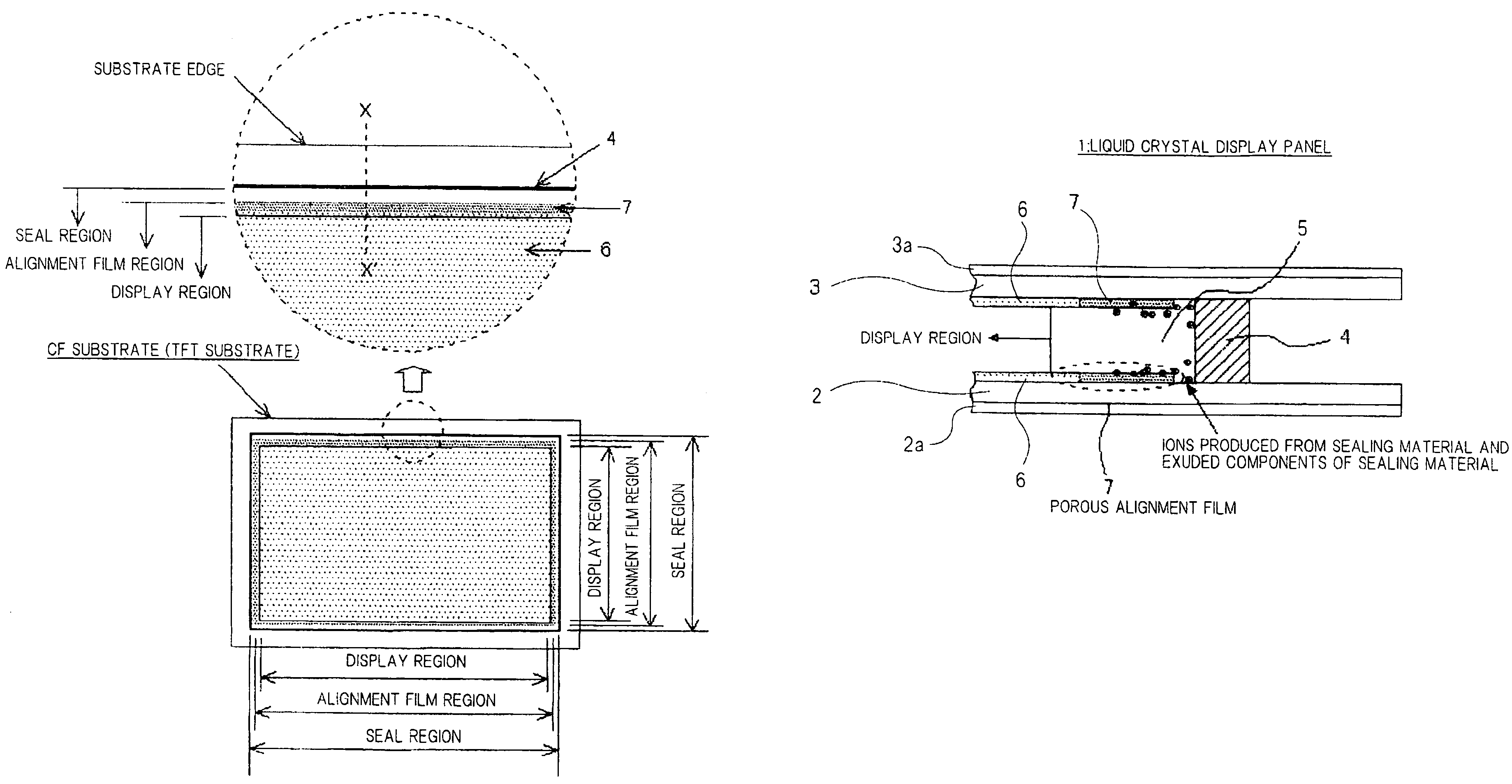
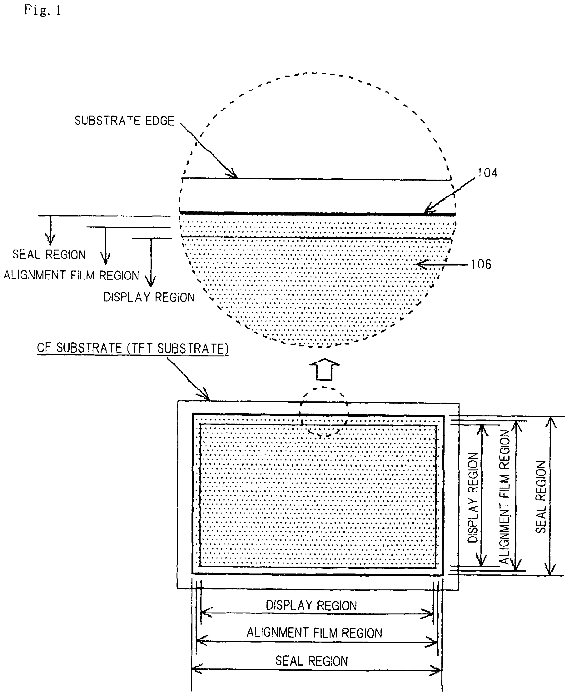
[0065]In general, a liquid crystal display panel has a TFT substrate formed with switching devices, such as TFTs, arranged in a matrix fashion, and a CF substrate formed with a black matrix, color filter (CF), and the like. Opposed faces of these substrates are each formed with an alignment film that is treated for alignment. A predetermined gap is defined between the two substrates by positioning insulating spacers, such as polymer beads or silica beads of a predetermined shape, or insulating columns of an acrylic resin or the like. Such a liquid crystal display panel displays an image by controlling the alignment direction of liquid crystal encapsulated in the gap by means of an electric field produced by electrodes formed on at least one substrate.

[0066]In order to fabricate a high-qua...

exemplary embodiment 2

[0081]Description will be made of a liquid crystal display device and a fabrication method thereof according to a second exemplary embodiment of the present invention with reference to FIG. 10.

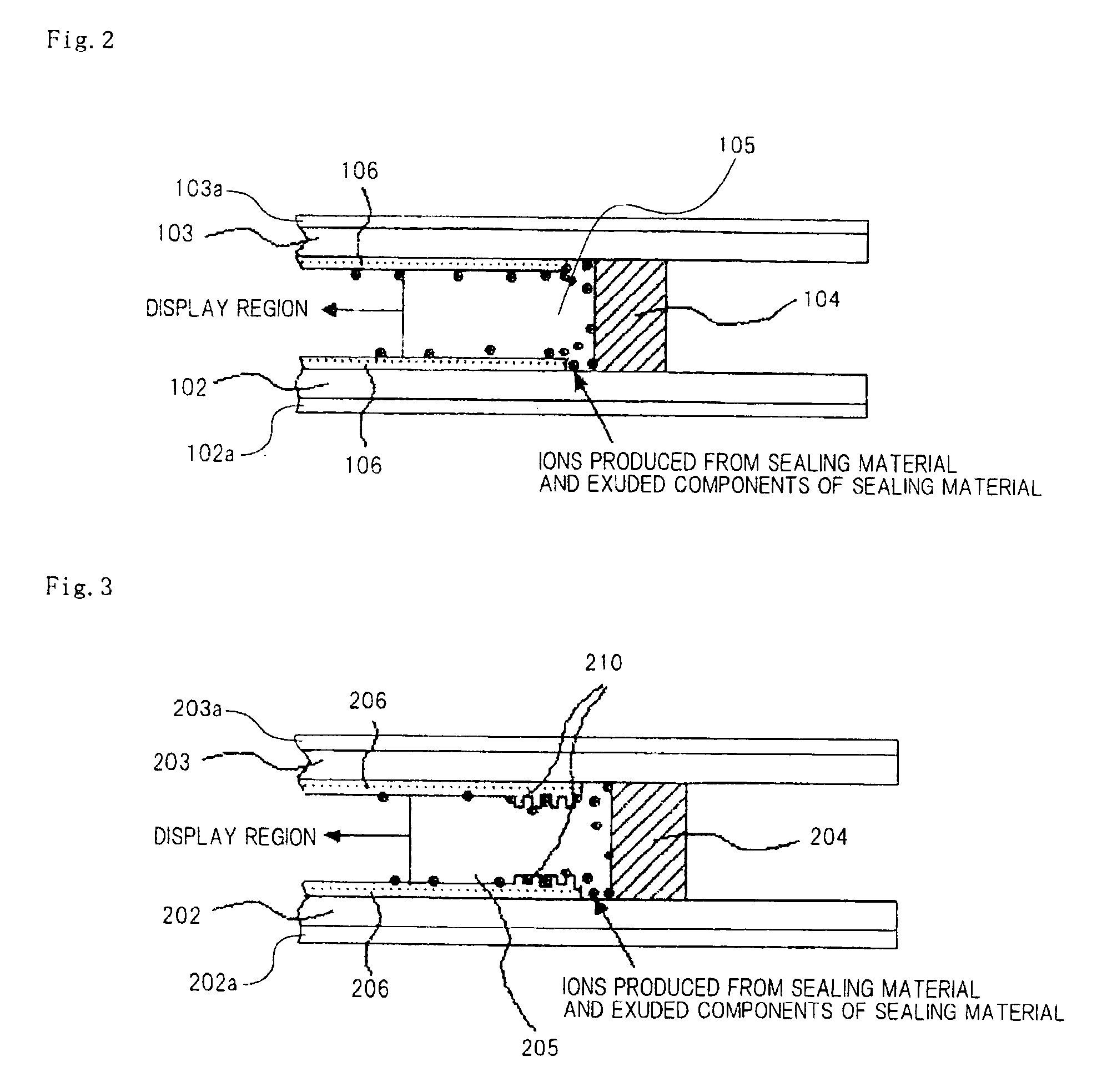
[0082]FIG. 10 is a schematic view illustrating a process from an alignment film application step to a plasma ashing step for fabricating a liquid crystal display panel according to the present exemplary embodiment.

[0083]In the alignment film application step, printing using an alignment plate was performed to apply the alignment material to surfaces of the TFT substrate and CF substrate, thus providing the display region and the region outside the display region with alignment films (step A in FIG. 10), in the same manner as in the first exemplary embodiment.

[0084]In the subsequent alignment film provisional drying step, leveling was performed at 80° C. for both the display region and the region outside the display region (step B in FIG. 10).

[0085]In the subsequent alignment film baking step, ...

exemplary embodiment 3

[0097]Description will be made of a liquid crystal display device and a fabrication method thereof according to a third exemplary embodiment of the present invention.

[0098]In the same manner as in the above-described second exemplary embodiment, the process from the alignment film application to the alignment film baking was performed to provide required alignment films in the display region and the region outside the display region.

[0099]In the subsequent plasma ashing step, the surface of each substrate except the region outside the display region was covered with a mask to allow the alignment film in the region outside the display region to be ashed locally. The entire substrate surface was directly irradiated with plasma by means of a fixed plasma head to form minute pores in the alignment film only in the region outside the display region. Thus, porous alignment films were formed.

[0100]Thereafter, in the rubbing step, rubbing was performed on the alignment film surfaces of the ...


PUM

PropertyMeasurementUnit
pore size diametersaaaaaaaaaa

Abstract

In applying an alignment material to surfaces of a CF substrate and a TFT substrate, which form a liquid crystal panel, to form alignment films, an alignment film is formed so as to cover at least a display region in which pixels are arranged in a matrix fashion, while a porous alignment film, which has a porous film structure with a higher impurity adsorptive property than the former alignment film, is formed in a region outside the former alignment film, for example, in a region intermediate the display region and a seal region surrounded by a sealing material, whereby the porous alignment film formed in the region outside the display region can efficiently adsorb contaminants, such as residual impurity ions produced from the sealing material and uncured components of the sealing material, to prevent the contaminants from penetrating into the display region and being fixed therein.

Description

[0001]This application is based upon and claims the benefit of priority from Japanese patent application No. 2007-105717, filed on Apr. 13, 2007, and Japanese patent application No. 2008-049315, filed on Feb. 29, 2008, the disclosure of which is incorporated herein in its entirety by reference.BACKGROUND OF THE INVENTION[0002]1. Field of the Invention[0003]The present invention relates to a liquid crystal display device and a method of fabricating the same. In particularl, the present invention relates to a liquid crystal display device characterized by an alignment film formed on a substrate surface, and a method of fabricating the same.[0004]2. Description of the Related Art[0005]Liquid crystal display devices are widely used as display devices for AV equipment and OA equipment in view of their advantages including slimness, lightness in weight, and low power consumption. Such a liquid crystal display device includes: a liquid crystal panel in which a liquid crystal is sandwiched ...

Claims


Application Information

Patent Timeline
Patent Type & Authority Patents(United States)
IPC IPC(8): G02F1/1337
CPCG02F1/1337G02F1/133711G02F1/1339
Inventor MOTOMATSU, TOSHIHIKOSUGIMOTO, MITSUHIRO
Owner NEC LCD TECH CORP
Why Eureka
Try Eureka