Method and structure for increased wire bond density in packages for semiconductor chips

a technology of semiconductor chips and wire bonds, applied in the direction of semiconductor devices, semiconductor/solid-state device details, electrical equipment, etc., can solve the problems of destroying device functionality, shortening of adjacent wires and pads, and increasing the number of i/o (input/output) connections and pads accordingly

Active Publication Date: 2011-02-08
TAIWAN SEMICON MFG CO LTD
View PDF6 Cites 3 Cited by
  • Summary
  • Abstract
  • Description
  • Claims
  • Application Information

AI Technical Summary

Problems solved by technology

Due to the increased complexity of each IC chip, the number of I / O (input / output) connections and pads also increases accordingly.
It is therefore a challenge to incorporate more input / output pads in a reduced area.
If the conventional, relatively thick bond wires are used and coupled to pads having a reduced pitch, the adjacent wires and pads can become shorted destroying device functionality.
Conversely, the use of smaller wires will result in poor electric performance, for example increased resistance, when such wires are coupled to pads of reduced dimensions.

Method used


Image

  • Method and structure for increased wire bond density in packages for semiconductor chips
  • Method and structure for increased wire bond density in packages for semiconductor chips
  • Method and structure for increased wire bond density in packages for semiconductor chips

Examples


Embodiment Construction

[0015]The present invention is directed to IC chips mounted in or on a semiconductor package and having bond pads thereon. The bond pads are electrically and physically coupled to contact pads on the package substrate via bond wires. The bond wires may be formed of the same or different materials and include different thicknesses. The semiconductor package may include one or more package substrates which may be stacked over one another in some embodiments.

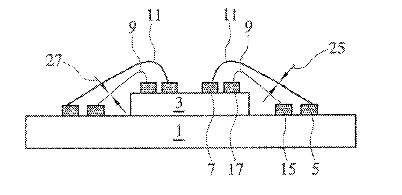
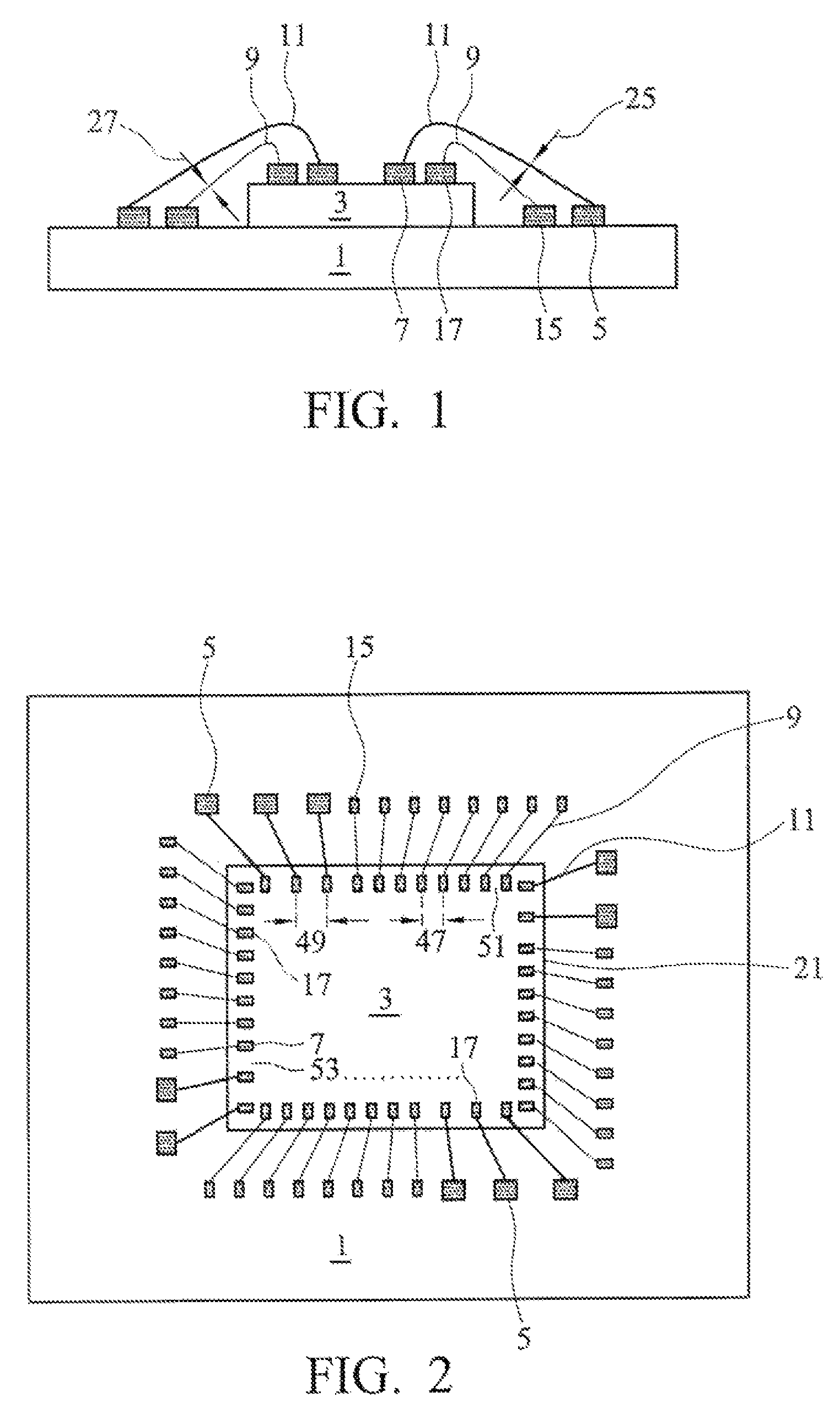
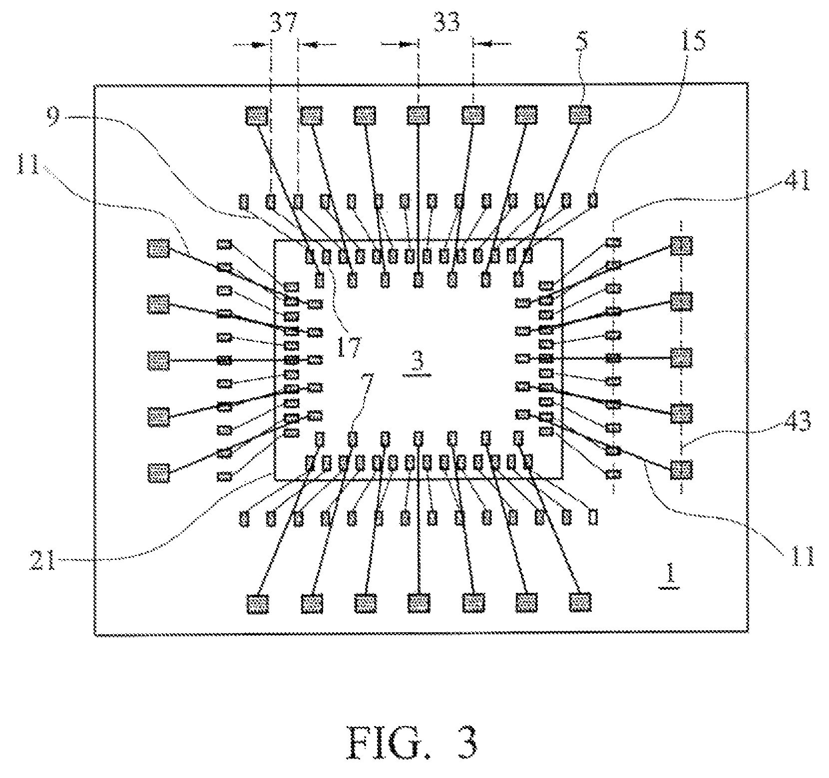
[0016]Referring to FIG. 1, IC chip 3 is mounted on package substrate 1 and is centrally disposed in the illustrated embodiment. According to other exemplary embodiments, IC chip 3 may be disposed in locations other than the center of package substrate 1. According to other exemplary embodiments, IC chip 3 may be disposed within a recess formed in package substrate 1. IC chip 3 includes an integrated circuit or semiconductor device that may carry out any of various functions.

[0017]IC chip 3 includes a plurality of bond pads which fu...


PUM


Abstract

A semiconductor package provides an IC chip on at least one package substrate and including signal bond pads, ground bond pads and power bond pads. The package substrate includes signal contact pads, ground contact pads and power contact pads which are respectively coupled to signal bond pads, ground bond pads and power bond pads formed on the IC chip. The contact pads are coupled to the associated bond pads by a bonding wire. The bonding wires that connect the power and ground pads have a thickness that is greater than the thickness of the bonding wires that couple the signal pads. The various bond pads on the IC chip may be staggered to provide for enhanced compactness and integration. The package substrates may be a plurality of stacked package substrates.

Description

FIELD OF THE INVENTION[0001]The present invention relates to semiconductor packages and assemblies and methods for forming the same.BACKGROUND[0002]IC (integrated circuit) chips are semiconductor or other suitable chips that have an integrated circuit formed thereon. IC chips have microscopic input / output pads through which the integrated circuit is coupled to the outside world. The IC chips must be assembled in packages or other structures before being coupled to external devices and used in various applications. In the rapidly-advancing semiconductor manufacturing industry, and in the electronics industry as well, there is a push to increase integration levels and decrease device sizes. This is reflected in smaller and more compact IC chips and smaller components that combine to form the electronic devices in which the IC chips are used. As such, the packages that accommodate the chips must be accordingly miniaturized. Due to the increased complexity of each IC chip, the number of...

Claims


Application Information

Patent Timeline
Patent Type & Authority Patents(United States)
IPC IPC(8): H01L23/49
CPCH01L23/5286H01L24/06H01L24/49H01L24/45H01L2224/04042H01L2224/05553H01L2224/05624H01L2224/05644H01L2224/32145H01L2224/45015H01L2224/45124H01L2224/45144H01L2224/45147H01L2224/48091H01L2224/48145H01L2224/4903H01L2224/49051H01L2224/49171H01L2224/49175H01L2224/49431H01L2924/01013H01L2924/01029H01L2924/01079H01L2924/01082H01L2924/14H01L2924/20751H01L2924/00014H01L24/48H01L2924/01033H01L2924/00H01L2224/48724H01L2224/48744H01L2224/48624H01L2224/48644H01L2224/48844H01L2224/48824H01L2224/023H01L2224/05554H01L2224/45099H01L2924/00015H01L2924/00012H01L2924/0001
Inventor CHEN, HSIEN-WEIHSU, SHIH-HSUN
Owner TAIWAN SEMICON MFG CO LTD
Why Eureka
Try Eureka