Signal line for a display device, etchant, thin film transistor panel, and method for manufacturing the same

a technology of thin film transistors and display devices, which is applied in static indicating devices, instruments, chemistry apparatuses and processes, etc., can solve the problems of poor physical and chemical characteristics of materials having low resistivity, deterioration of reliability of signal lines, and easy contact with other materials, so as to achieve low line resistance and reliability, and increase reliability , the effect of low resistan

Active Publication Date: 2011-02-15
SAMSUNG DISPLAY CO LTD
View PDF22 Cites 9 Cited by
  • Summary
  • Abstract
  • Description
  • Claims
  • Application Information

AI Technical Summary

Benefits of technology

[0010]The present invention provides a thin film transistor (“TFT”) array and a method for manufacturing the same to achieve low line resistance and reliability for the material of the signal lines. The present invention also provides a signal line for a display device having low line resistance and increased reliability, and an etchant for use in the manufacture of a display device having the signal line.

Problems solved by technology

However, the material having low resistivity has poor physical and chemical characteristics such as against external impact and durability such that its contact with other materials is easily corroded.
Furthermore, remnants and skews are greatly generated in a manufacturing process using the materials such that the reliability for the material of the signal lines is deteriorated.

Method used


Image

  • Signal line for a display device, etchant, thin film transistor panel, and method for manufacturing the same
  • Signal line for a display device, etchant, thin film transistor panel, and method for manufacturing the same
  • Signal line for a display device, etchant, thin film transistor panel, and method for manufacturing the same

Examples


Embodiment Construction

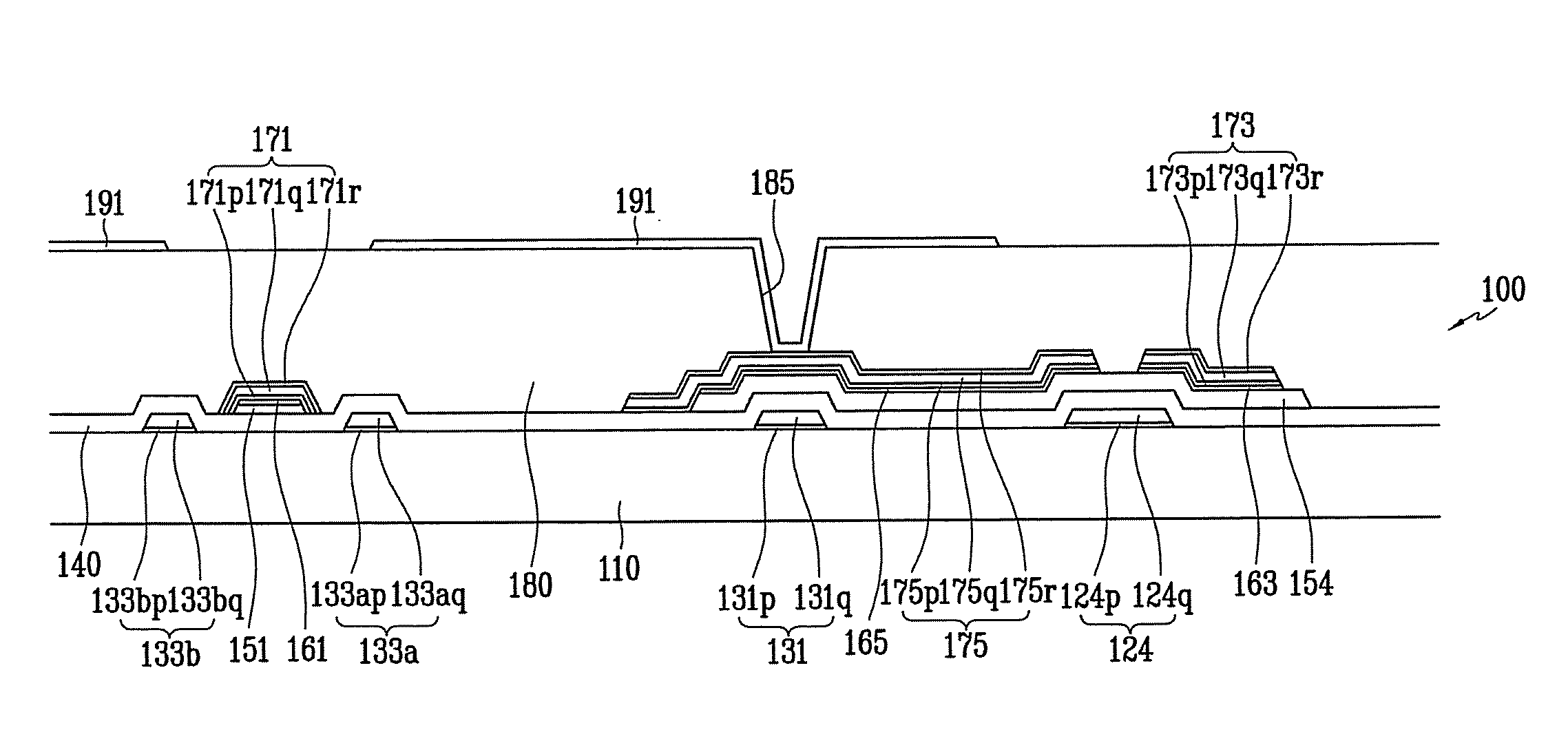
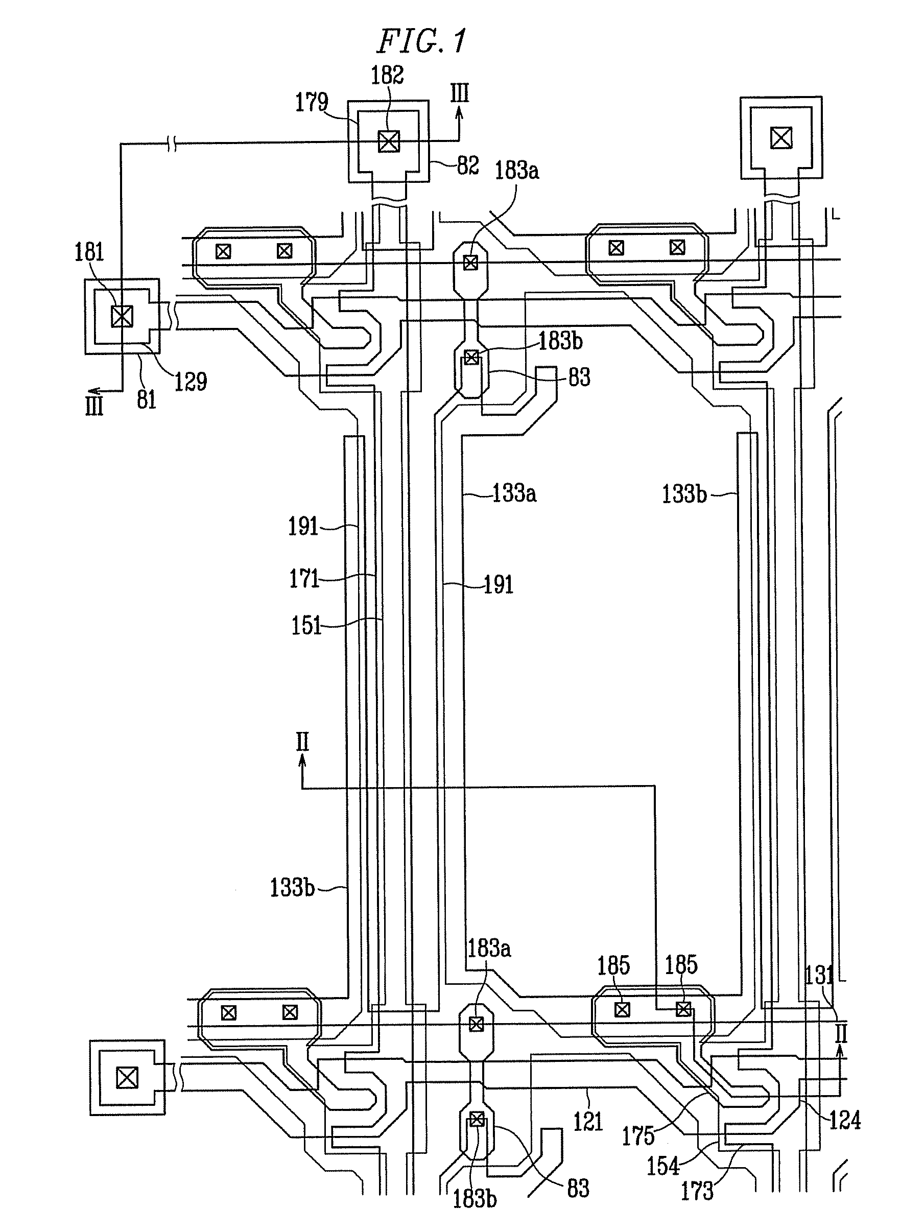
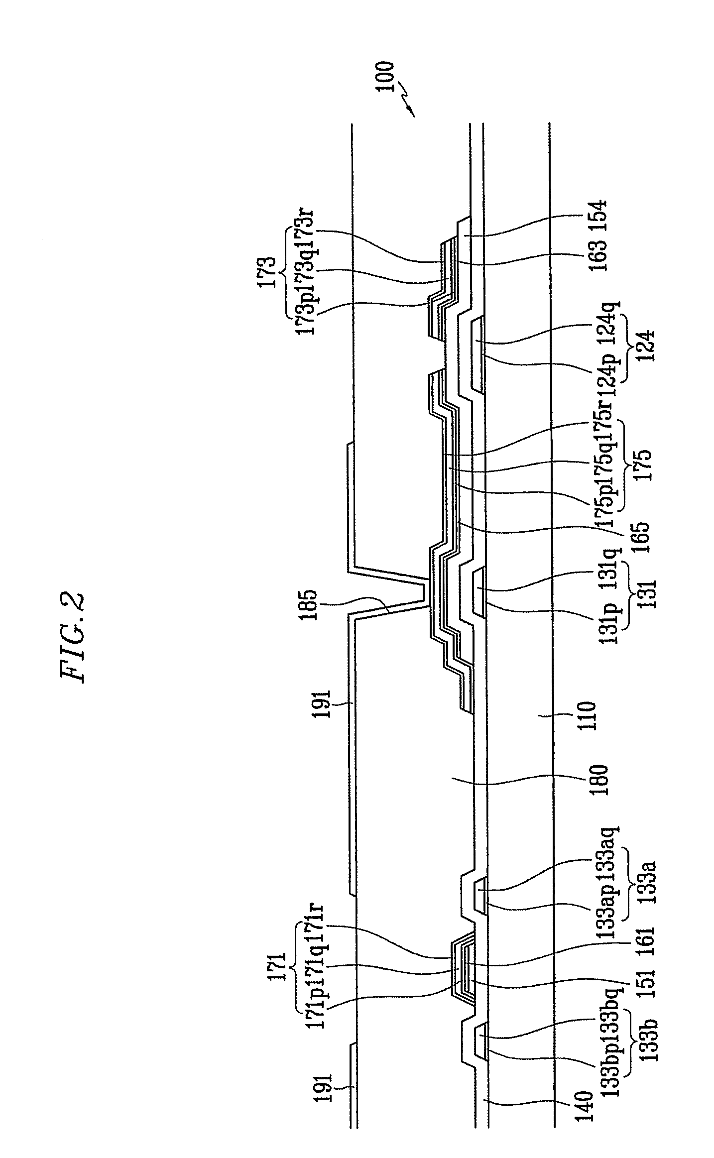
[0039]The present invention will be described more fully hereinafter with reference to the accompanying drawings, in which preferred and exemplary embodiments of the invention are shown. The present invention may, however, be embodied in many different forms and should not be construed as limited to the embodiments set forth herein. Rather, these embodiments are provided so that this disclosure will be thorough and complete, and will fully convey the scope of the invention to those skilled in the art.

[0040]In the drawings, the thickness of layers, films, and regions are exaggerated for clarity. Like numerals refer to like elements throughout. It will be understood that when an element such as a layer, film, region, or substrate is referred to as being “on” another element, it can be directly on the other element or intervening elements may also be present. In contrast, when an element is referred to as being “directly on” another element, there are no intervening elements present. A...


PUM


Abstract

A thin film panel includes a substrate, a gate line formed on the substrate, a gate insulating layer formed on the gate line, a semiconductor layer formed on the gate insulating layer, a data line, including a source electrode, and a drain electrode formed on the gate insulating layer or the semiconductor layer, and a pixel electrode connected to the drain electrode, wherein at least one of the gate line and the data line and drain electrode includes a first conductive layer made of a molybdenum Mo-niobium Nb alloy and a second conductive layer made of a copper Cu-containing metal.

Description

[0001]This application claims priority to Korean patent application No. 10-2006-0095979, filed on Sep. 29, 2006, and all the benefits accruing therefrom under 35 U.S.C. §119, the contents of which in its entirety are herein incorporated by reference.BACKGROUND OF THE INVENTION[0002](a) Field of the Invention[0003]The present invention relates to a signal line for a display device, etchant, thin film transistor panel, and a method for manufacturing the same. More particularly, the present invention relates to a signal line for a display device having low line resistance and increased reliability, etchant, thin film transistor panel, and a method for manufacturing the same.[0004](b) Description of the Related Art[0005]Generally, a flat panel display such as a liquid crystal display (“LCD”), an organic light emitting diode (“OLED”) display, and an electrophoretic display includes a pair of electric-field generating electrodes and an electro-optical active layer disposed therebetween. T...

Claims


Application Information

Patent Timeline
Patent Type & Authority Patents(United States)
IPC IPC(8): H01L21/00
CPCC09K13/08H01L27/124H01L29/4908G09G2300/0426G09G2300/0439G09G2320/0223H01L2924/0002H01L23/53238H01L2924/00G02F1/136
Inventor PARK, HONG-SICKKIM, BONG-KYUNJEONG, CHANG-OHCHOUNG, JONG-HYUNHONG, SUN-YOUNGSHIN, WON-SUKLEE, BYEONG-JIN
Owner SAMSUNG DISPLAY CO LTD
Why Eureka
Try Eureka