Unlock instant, AI-driven research and patent intelligence for your innovation.

Method of forming floating gate, non-volatile memory device using the same, and fabricating method thereof

a non-volatile memory and floating gate technology, applied in the direction of semiconductor devices, electrical devices, nanotechnology, etc., can solve the problems of difficult to adjust or control the number of charge defects inside the nitride film to capture electrons, and the film quality characteristic of each component,

Active Publication Date: 2011-03-01
KOOKMIN UNIV IND ACAD COOP FOUND
View PDF5 Cites 5 Cited by
  • Summary
  • Abstract
  • Description
  • Claims
  • Application Information

AI Technical Summary

Benefits of technology

[0020]To overcome inconveniences of the conventional art, it is an object of the present invention to provide a method of forming a floating gate, a non-volatile memory device using the same, and a method of fabricating the non-volatile memory device, in which metal nano-crystals of nano-size whose density and size are easily controlled and which are self-assembled using micelle templates, is used as a floating gate of a non-volatile memory device.
[0021]It is another object of the present invention to provide a method of forming a floating gate, a non-volatile memory device using the same, and a method of fabricating the non-volatile memory device, in which the floating gate can be formed using metal nano-crystals without seeking a high-temperature heat treatment process which may raise a problem such as a change in a membranous feature.
[0044]As described above, according to the present invention, a floating gate of a non-volatile memory device can be formed of metal nano-crystals of nano-size, a density of the metal nano-crystals forming the floating gate can be controlled, and the metal nano-crystals of nano-size can be formed into the floating gate without having a high-temperature heat treatment process.

Problems solved by technology

Non-volatile memory devices have a substantially limitless cumulative capacity, respectively.
However, it is hard to adjust or control the number of the charge defects of the inside of the nitride film to capture electrons.
However, when a high-temperature heat treatment process proceeds to form nano-crystals in a silicon substrate, a film quality characteristic of each component (for example, a tunnel oxide film) may change according to an interface reaction and defect.
Problems such as components of various film qualities and unnecessary diffusion of ions due to an ion implantation process may occur, to thus deteriorate characteristics of the components.
However, no method of solving a problem which may be caused by a high-temperature heat treatment process while using nano-crystals as a floating gate is disclosed or taught.

Method used


Image

  • Method of forming floating gate, non-volatile memory device using the same, and fabricating method thereof
  • Method of forming floating gate, non-volatile memory device using the same, and fabricating method thereof
  • Method of forming floating gate, non-volatile memory device using the same, and fabricating method thereof

Examples


Embodiment Construction

[0054]Hereinbelow, a method of forming a floating gate, a non-volatile memory device using the same, and a method of fabricating the non-volatile memory device according to the present invention will be described with reference to the accompanying drawings. Like reference numerals are assigned for like elements in the drawings. Here, the present invention will be described using a flash memory device among non-volatile memory devices as an example, but can be applied to the other non-volatile memory devices.

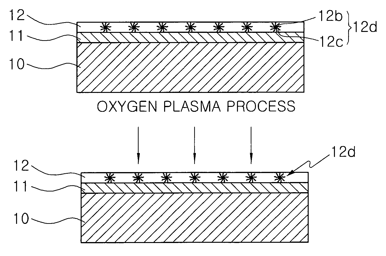
[0055]FIGS. 1A to 1H are cross-sectional views for explaining a method of manufacturing a non-volatile memory device according to a preferable embodiment of the present invention, respectively.

[0056]Referring to FIG. 1A, a tunnel oxide film 11 is formed on a silicon substrate 10 that is a semiconductor substrate. The tunnel oxide film 11 is formed on an active area of the silicon substrate 10 that is divided into a field area and the active area. Here, it is preferable that the t...


PUM


Abstract

Provided is a method of forming a floating gate, a non-volatile memory device using the same, and a method of fabricating the non-volatile memory device, in which nano-crystals of nano-size whose density and size can be easily adjusted, are synthesized using micelles so as to be used as the floating gate of the non-volatile memory device. The floating gate is fabricated by forming a tunnel oxide film on the semiconductor substrate, coating a gate formation solution on the tunnel oxide film in which the gate formation solution includes micelle templates into which precursors capable of synthesizing metallic salts in nano-structures formed by a self-assembly method are introduced, and arranging the metallic salts on the tunnel oxide film by removing the micelle templates, to thereby form the floating gate.

Description

CROSS-REFERENCE TO RELATED APPLICATION[0001]This application claims the benefit of Korean Patent Application No. 10-2007-0030850, filed on Mar. 29, 2007, in the Korean Intellectual Property Office, the disclosure of which is incorporated herein by reference.BACKGROUND OF THE INVENTION[0002]1. Field of the Invention[0003]The present invention relates to a method of forming a floating gate, a non-volatile memory device using the same, and a method of fabricating the non-volatile memory device. More particularly, the present invention relates to a method of forming a floating gate, a non-volatile memory device using the same, and a method of fabricating the non-volatile memory device, in which the floating gate which uses nano-crystals of nano-size whose density and size can be easily adjusted, is formed and the nano-crystals are formed using micelles without seeking heat treatment of high-temperature, so that a high-temperature heat treatment process that may raise a problem such as a...

Claims


Application Information

Patent Timeline
Patent Type & Authority Patents(United States)
IPC IPC(8): H01L21/336
CPCB82Y10/00H01L21/28273H01L29/42324H01L29/513H01L29/40114H01L29/66825
Inventor LEE, JAEGABLEE, JANG-SIKLEE, CHI YOUNGSOHN, BYEONG HYEOK
Owner KOOKMIN UNIV IND ACAD COOP FOUND