Method for fabricating a fin-shaped semiconductor structure and a fin-shaped semiconductor structure

a technology of semiconductor structure and fin, which is applied in the direction of semiconductor devices, basic electric elements, electrical equipment, etc., can solve the problems of high current density as compared to conventional devices, and achieve the effects of enhancing the transport capability of fin-shaped structures, enhancing “three-dimensional” semiconductor devices, and increasing charge transport performan

Active Publication Date: 2011-03-08
INFINEON TECH AG
View PDF5 Cites 9 Cited by
  • Summary
  • Abstract
  • Description
  • Claims
  • Application Information

AI Technical Summary

Benefits of technology

[0004]According to one embodiment of the present invention, a fin-shaped structure of a semiconductor material is used, which is under tensile stress along a longitudinal direction of the fin-shaped structure. The longitudinal direction is intended to be the direction of the charge transport. Therefore, the charge transport performance is increased within the fin-shaped structure, allowing the building of enhanced “three-dimensional” semiconductor devices.
[0005]According to a further embodiment of the present invention, a method for fabricating a fin-shaped semiconductor structure is provided. A fin-shaped structure is formed from a semiconductor material. The fin-shaped structure is processed to generate a tensile stress within the semiconductor material along a longitudinal direction of the fin. Therefore, when a charge transport takes place in the longitudinal direction, the transport capabilities of the fin-shaped structures are significantly enhanced, allowing the construction of more efficient devices.

Problems solved by technology

However, the smaller the geometry of the devices, the higher the current-densities as compared to conventional devices.

Method used


Image

  • Method for fabricating a fin-shaped semiconductor structure and a fin-shaped semiconductor structure
  • Method for fabricating a fin-shaped semiconductor structure and a fin-shaped semiconductor structure
  • Method for fabricating a fin-shaped semiconductor structure and a fin-shaped semiconductor structure

Examples


Embodiment Construction

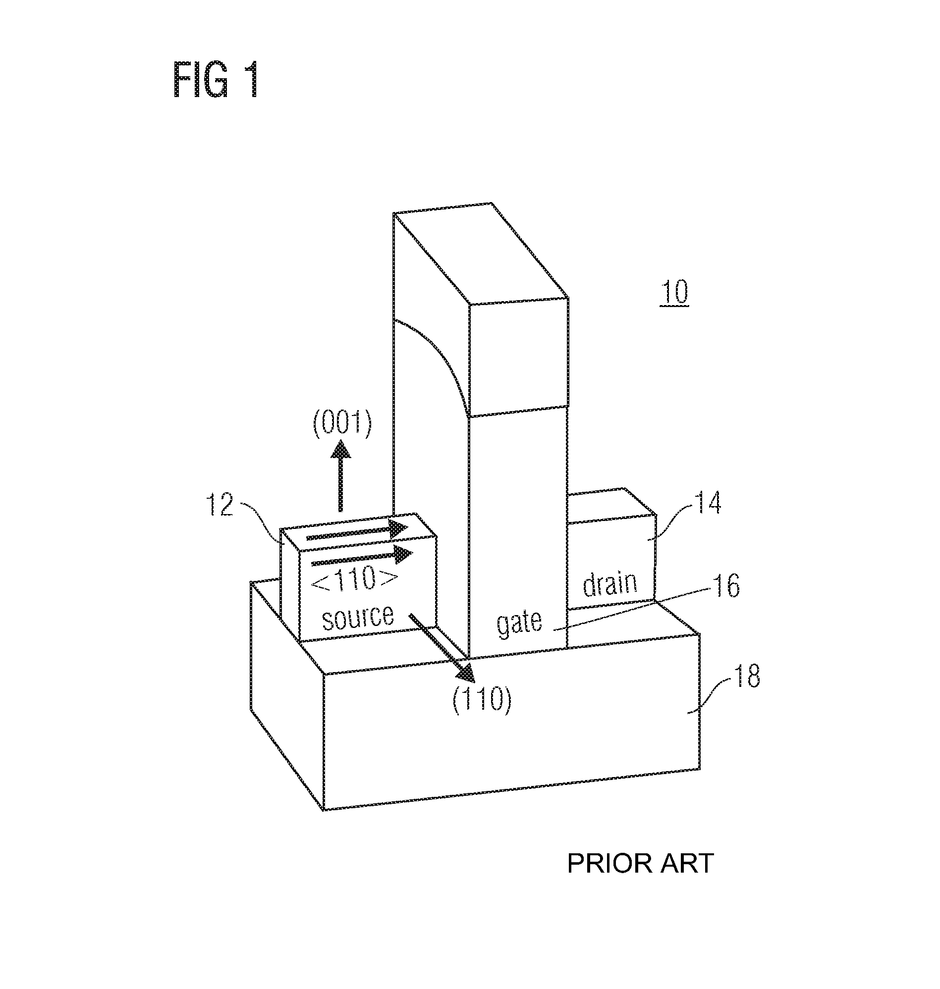
[0014]Prior to a detailed discussion of several embodiments of the present invention, FinFETS implementing fin-shaped semiconductor structures are shortly reviewed referencing FIGS. 1 and 2, to provide a better understanding of the inventive concept, directed to the fabrication or use of fin-shaped semiconductor structures. It goes without saying that, although the invention will mainly be described by the creation of FinFETs within the following paragraphs, the invention may appropriately apply also to other semiconductor devices which require fin-shaped semiconductor structures or which may benefit from the application of fin-shaped semiconductor structures.

[0015]FIG. 1 shows a principle sketch of a FinFET device 10, having a source region 12, a drain region 14 and a gate region 16, which are built on a support substrate 18. Opposed to conventional FETs using planar geometries, FinFETs transport current from the source region 12 to the drain region 14 through a channel volume exte...


PUM


Abstract

A fin-shaped structure is formed from a semiconductor material. The fin-shaped structure is processed to generate a tensile strain within the semiconductor material along a longitudinal direction of the fin.

Description

BACKGROUND[0001]The present invention relates to fin-shaped semiconductor structures and a method for fabricating the same, and in particular to a concept as to how to enhance the electrical properties of fin-shaped semiconductor structures.[0002]The demand for ever smaller semiconductor structures led to the development of three-dimensional structures, deviating from simple planar geometries, as for example, to the development of FinFET devices.[0003]However, the smaller the geometry of the devices, the higher the current-densities as compared to conventional devices. Ongoing shrinkage of the structures in semiconductor processing also requires an enhancement of the conduction probabilities of the semiconductor materials used. One related technique is using so-called “strained-silicon,” which is silicon with artificially increased or decreased lattice coefficients in the direction of the charge carrier transport, such that the carrier mobility increases. A device using such straine...

Claims


Application Information

Patent Timeline
Patent Type & Authority Patents(United States)
IPC IPC(8): H01L21/00
CPCH01L29/045H01L29/66545H01L29/66795H01L29/7843H01L29/785H01L29/7845
Inventor STAPELMANN, CHRISSCHULZ, THOMAS
Owner INFINEON TECH AG
Why Eureka
Try Eureka