Deposition-plasma cure cycle process to enhance film quality of silicon dioxide

a technology of depositionplasma and cure cycle, applied in the field of depositionplasma cure cycle process to enhance the film quality of silicon dioxide, can solve the problems of difficult to completely fill gaps and trenches in these structures without creating, too much electrical noise, and difficult to completely fill gaps and trenches in these structures, so as to reduce the carbon content in the layer

Active Publication Date: 2011-03-08
APPLIED MATERIALS INC
View PDF168 Cites 51 Cited by
  • Summary
  • Abstract
  • Description
  • Claims
  • Application Information

AI Technical Summary

Problems solved by technology

While the ability to make device structures with ever increasing aspect ratios has allowed more of the structures (e.g., transistors, capacitors, diodes, etc.) to be packed onto the same surface area of a semiconductor chip substrate, it has also created fabrication problems.
Once of these problems is the difficulty of completely filling the gaps and trenches in these structures without creating a void or seam during the filling process.
If the gaps were left empty, there would be too much electrical noise, and current leakage for the devices to operate properly (or at all).
As aspect ratios increased however, it became more difficult to fill the deep, narrow trench without having a blockage start a void or seam in the fill volume.
Voids and seams in a dielectric layer cause create problems both during semiconductor device fabrication and in the finished devices.
This results in unpredictable and inconsistent post-deposition processing of the layer, such as even etching, polishing, annealing, etc.
This can result in uneven, and inferior device performance due to electrical crosstalk, charge leakage, and even shorting within and between device elements.
Unfortunately however, slowing the deposition rate means increasing the deposition time, which reduces processing efficiency and production rates.
Unfortunately however, increasing the moisture level during a silicon oxide deposition can also adversely effect the properties of the deposited film, including its density (i.e., an increased wet etch rate ratio (WERR)) and dielectric properties (i.e., an increased k-value).

Method used


Image

  • Deposition-plasma cure cycle process to enhance film quality of silicon dioxide
  • Deposition-plasma cure cycle process to enhance film quality of silicon dioxide
  • Deposition-plasma cure cycle process to enhance film quality of silicon dioxide

Examples


Embodiment Construction

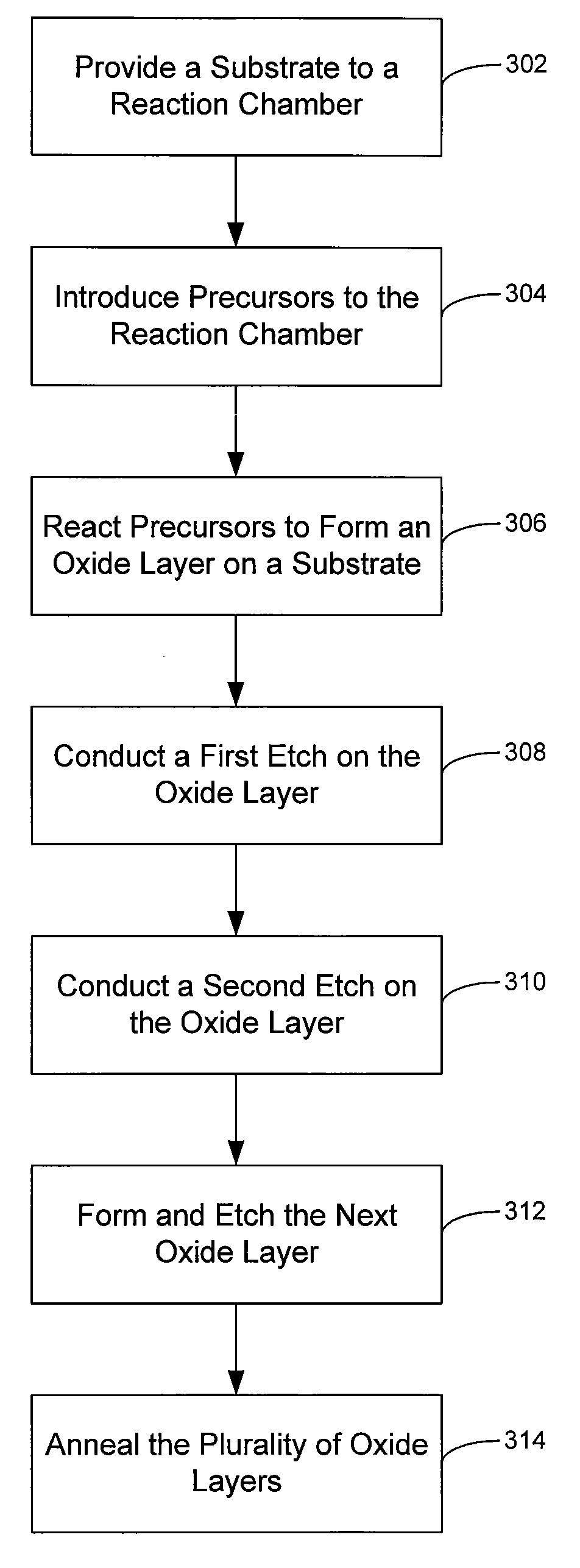
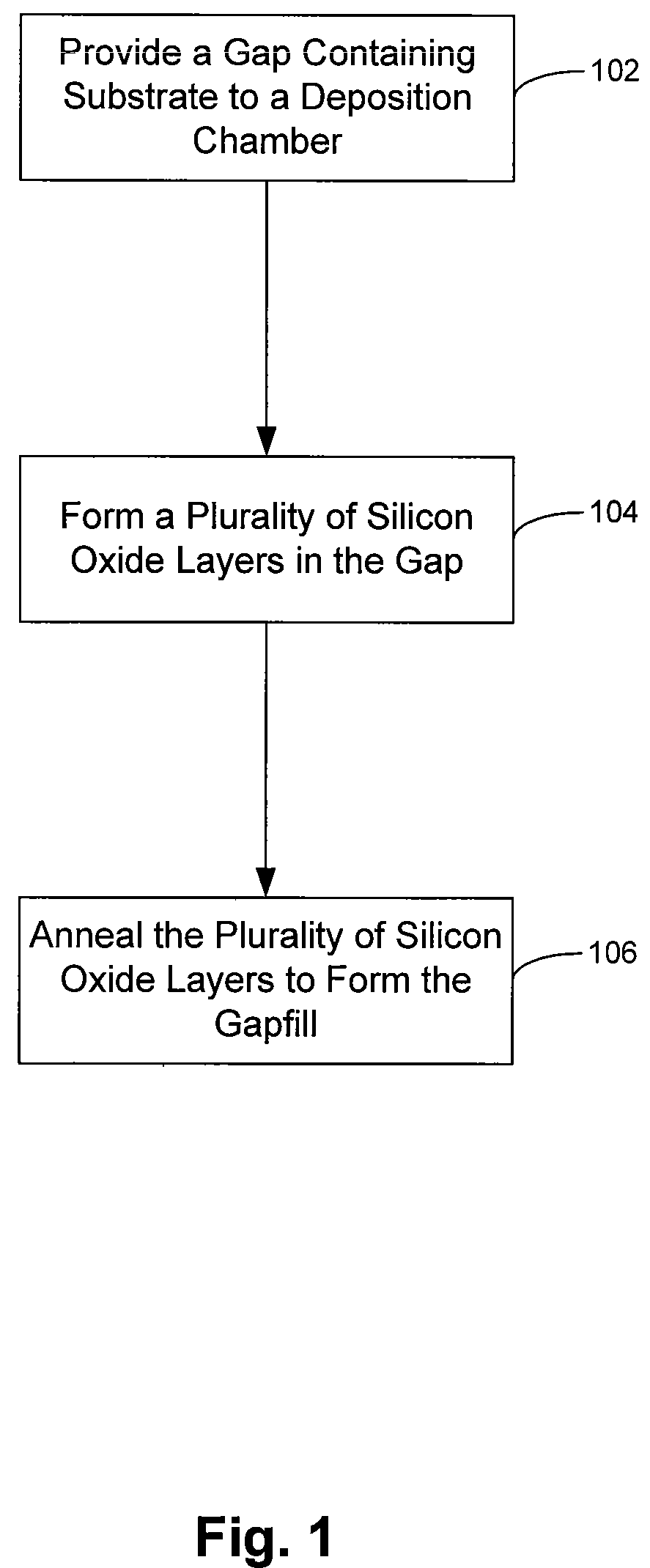
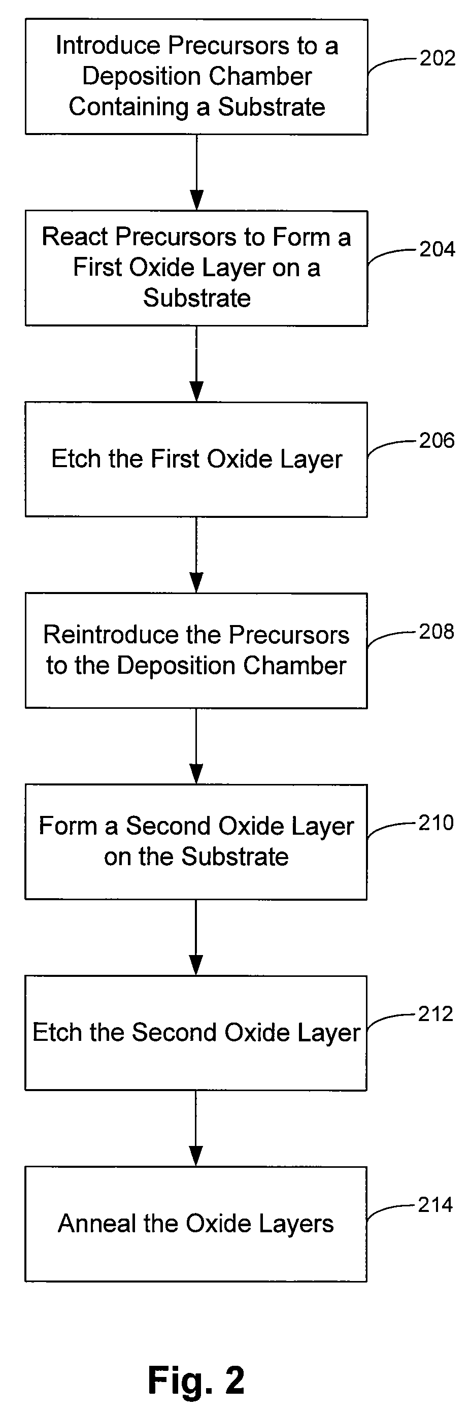
Systems and methods are described for multilayer, multicycle depositions of silicon oxide in gaps and on surfaces of a wafer substrate. Each oxide layer is thin enough (e.g., about 50 Å to about 300 Å) to allow an etch process to dissociate and remove impurities such as organic and hydroxyl groups that can adversely effect the quality and dielectric properties of the film. When a plurality of the oxide layers have been deposited and etched, an anneal may be done to form the layers into a high-quality, low-k silicon oxide film.

The silicon oxide may be formed from a reaction of highly reactive atomic oxygen and an organo-silicon precursor, such as OMCATS. The atomic oxygen may first be generated outside the chamber were the deposition occurs, and kept isolated from the organo-silicon precursor until they are mixed in the chamber. The resulting silicon oxide is carbon rich and highly flowable, providing a deposition film that easily flows to the bottoms of narrow gaps and trenches. Aft...


PUM

PropertyMeasurementUnit
temperatureaaaaaaaaaa

Abstract

Methods of filling a gap on a substrate with silicon oxide are described. The methods may include the steps of introducing an organo-silicon precursor and an oxygen precursor to a deposition chamber, reacting the precursors to form a first silicon oxide layer in the gap on the substrate, and etching the first silicon oxide layer to reduce the carbon content in the layer. The methods may also include forming a second silicon oxide layer on the first layer, and etching the second layer to reduce the carbon content in the second layer. The silicon oxide layers are annealed after the gap is filled.

Description

BACKGROUND OF THE INVENTIONAs the device density on integrated circuits continues to increase, the size and distance between device structures continue to decrease. The narrower widths in the gaps of the structures and the trenches between structures increases the ratio of height to width (i.e., the aspect ratio) in these formations. In other words, the continued miniaturization of integrated circuit elements is shrinking the horizontal width within and between these elements faster than their vertical height.While the ability to make device structures with ever increasing aspect ratios has allowed more of the structures (e.g., transistors, capacitors, diodes, etc.) to be packed onto the same surface area of a semiconductor chip substrate, it has also created fabrication problems. Once of these problems is the difficulty of completely filling the gaps and trenches in these structures without creating a void or seam during the filling process. Filling gaps and trenches with dielectri...

Claims


Application Information

Patent Timeline
Patent Type & Authority Patents(United States)
IPC IPC(8): H01L21/302
CPCC23C16/045C23C16/402H01L21/02126H01L21/02216H01L21/02274H01L21/0234H01L21/3105H01L21/31633
Inventor CHEN, XIAOLINNEMANI, SRINIVAS D.VENKATARAMAN, SHANKAR
Owner APPLIED MATERIALS INC
Why Eureka
Try Eureka