Metallized polyimide film

a polyimide film, metalized technology, applied in the direction of plasma technique, water-setting substance layered product, synthetic resin layered product, etc., can solve the problems of poor dimensional stability of the adhesive layer, inability to fully satisfy the demands of even thinner films, and difficulty in ultra fine processing of circuit boards. achieve the effect of superior bonding strength and large bonding strength

Inactive Publication Date: 2004-07-27
MITSUBISHI SHINDOH CO LTD
View PDF10 Cites 19 Cited by
  • Summary
  • Abstract
  • Description
  • Claims
  • Application Information

AI Technical Summary

Benefits of technology

According to this type of metallized polyimide film, a suitable degree of surface roughening treatment is performed on the surface of the polyimide film, and a film of molybdenum, silicon or silicon monoxide is then formed thereon with a suitable distribution, and consequently the bonding strength of the metal layer can be improved.
The material for the polyimide film 1 may utilize any polyimide resin typically used for this type of application, and both BPDA type polyimide resins and PMDA type polyimide resins are suitable. Generally, polyimide films using BPDA (biphenyltetracarboxylic acid) as a raw material (such as the commercial product "Upilex" manufactured by Ube Industries) offer superior dimensional stability under heat and moisture absorption, as well as excellent rigidity, and are mainly used for TAB applications, although the bonding strength of these polyimide films with metallic thin films is low. In contrast, polyimide films using PMDA (pyromellitic dianhydride) as a raw material (such as the commercial product "Kapton" manufactured by DuPont-Toray Co., Ltd., or the commercial product "Apical" manufactured by Kaneka Corporation) offer good bonding strength with metallic thin films.
According to a metallized polyimide film described above and a method of producing such a film, the bonding strength between the polyimide film 1 and the metal layer 4 can be increased, and this superior bonding strength can be maintained following durability tests. Furthermore, a large bonding strength can be achieved regardless of whether the interface contacting the intermediate layer 2 is a BPDA type polyimide or a PMDA type polyimide.

Problems solved by technology

However, in order to increase the packaging density in electronic devices, it is desirable to reduce the film thickness of this type of circuit board even further, and the structure described above, in which copper foil is bonded to a substrate, is unable to fully satisfy these demands for even thinner films.
Furthermore, in the aforementioned circuit boards using an adhesive, (1) the etching solution for the copper foil may penetrate through to the adhesive layer, and when a bias is then applied under conditions of high temperature and high humidity, copper migration may occur, causing a short circuit within the circuit, (2) in order to improve speed, the impedance must be matched and cross-talk reduced, but the presence of the adhesive makes this difficult, (3) the dimensional stability of the adhesive layer is poor, (4) the presence of the adhesive layer makes ultra fine processing of the circuit board difficult, making a shift to higher densities problematic, (5) the thermal characteristics of the adhesive layer are inferior to those of the plastic substrate material, leading to problems of thermal stability, and making a shift to higher densities problematic, and (6) the presence of the adhesive means that deformation of the product is more likely to occur.
However, in these types of structures, the post processes such as the circuit pattern formation process and the electroplating process cause a reduction in the bonding strength between the plastic substrate and the metallic thin film, increasing the possibility of the metallic thin film separating from the substrate.
However, none of the above methods is able to completely prevent the separation of the copper layer from the polyimide film, and a configuration capable of further strengthening the bonding between the copper layer and the polyimide film has been keenly sought.

Method used


Image

  • Metallized polyimide film
  • Metallized polyimide film
  • Metallized polyimide film

Examples


example 1

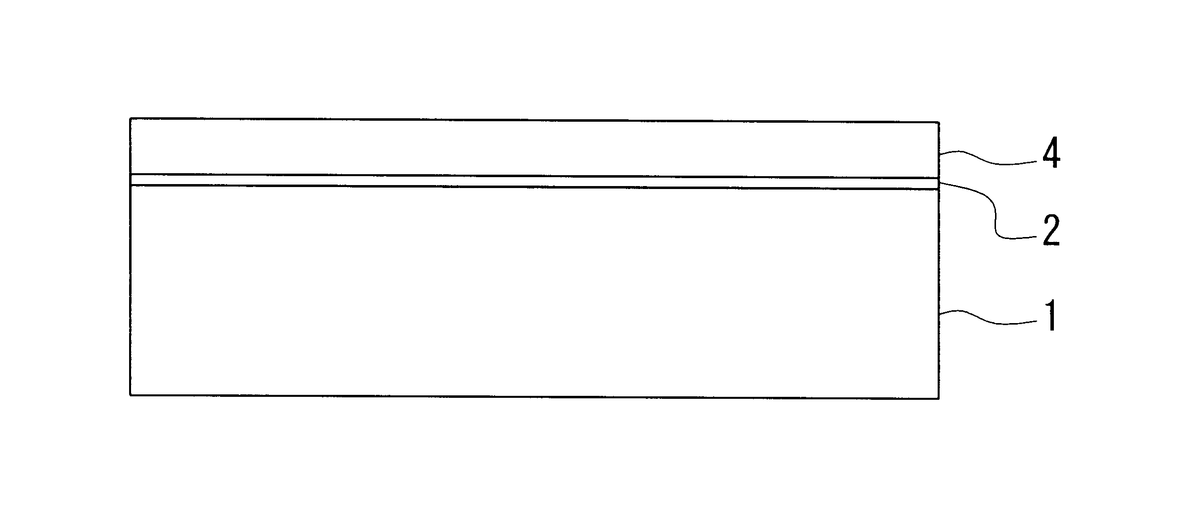
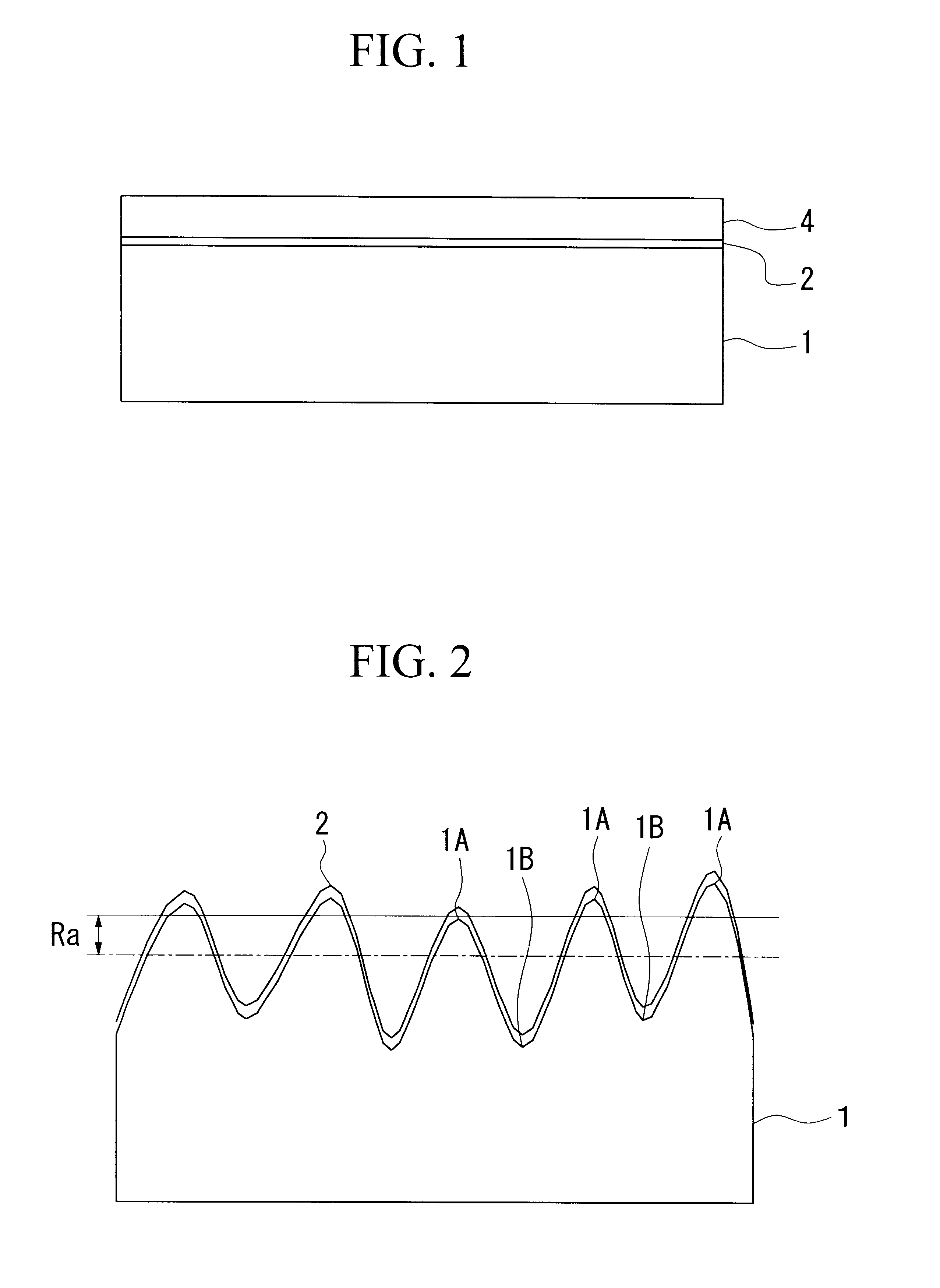
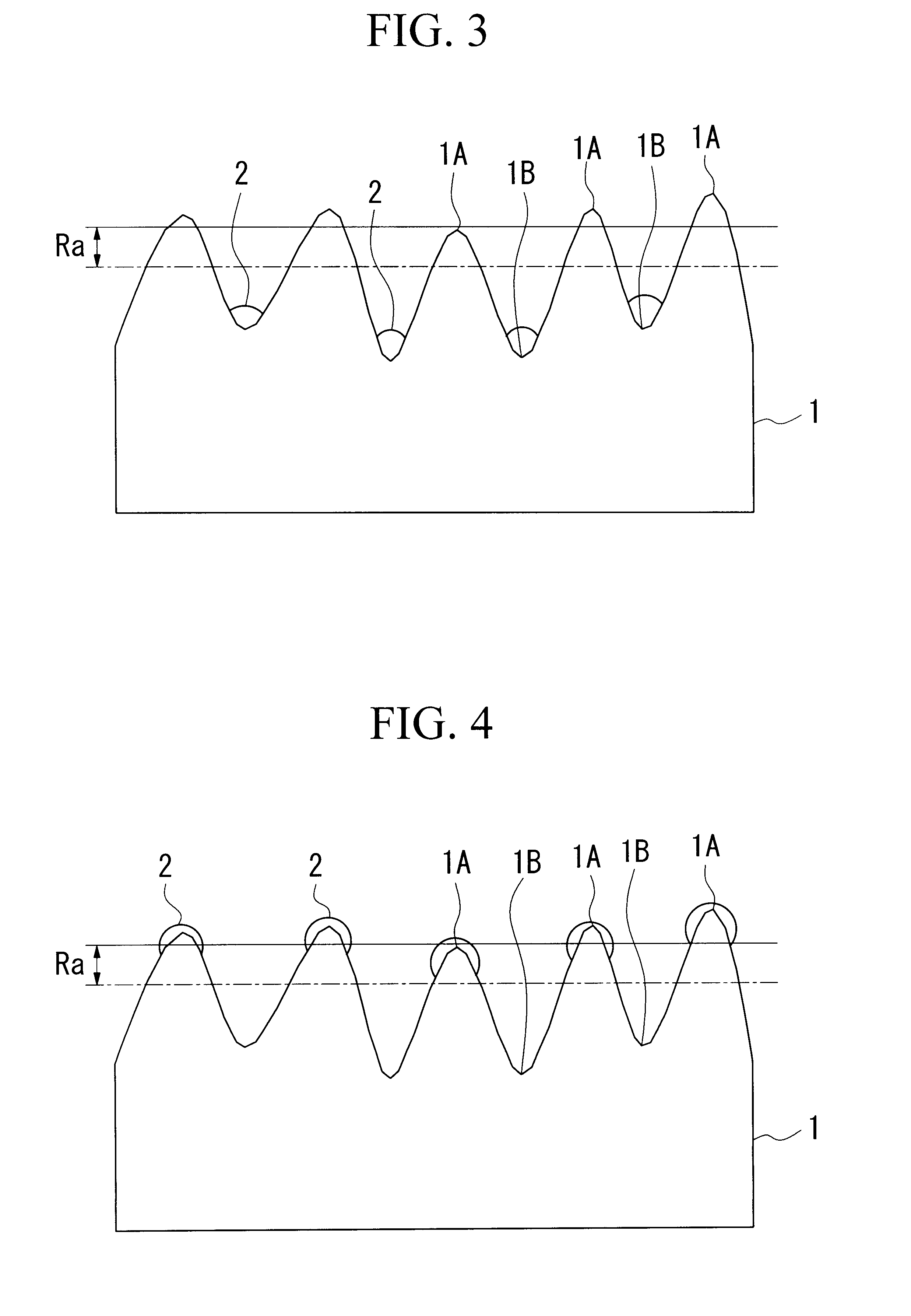
The commercial product "Upilex S" (thickness 50 .mu.m) manufactured by Ube Industries was used as a BPDA type polyimide film material, and this film material was subjected to plasma treatment using argon gas, under conditions including a radio frequency of 0.4 W / cm.sup.2 and a treatment time of 5 minutes. The Ra value for the film material following this treatment was 2.73 nm.

This surface treated film was then set inside a sputtering apparatus, and an intermediate layer and a metal layer were formed on the plasma treated surface under the conditions described below.

Intermediate layer material: molybdenum

Film formation conditions: argon gas, high frequency output 200 W

Film thickness: 1 nm=36.6% of the Ra value (2.73 nm)

Metal layer material: copper

Film formation conditions: argon gas, high frequency output 200 W

Film thickness: 300 nm

A copper sulfate bath was then used to form a 20 .mu.m electroplated layer of copper on the metal surface of the metallic thin film, thereby obtaining a m...

example 2

The commercial product "Kapton II" (thickness 50 .mu.m) manufactured by DuPont-Toray Co., Ltd. was used as a PMDA type polyimide film material, and by performing treatment in the same manner as the example 1, a metallized polyimide film of the example 2 was obtained. The Ra value following surface treatment was 2.93 nm (and consequently the thickness of the intermediate layer was 34.1% of the Ra value).


PUM

PropertyMeasurementUnit
Raaaaaaaaaaa
thicknessaaaaaaaaaa
thicknessaaaaaaaaaa

Abstract

A metallized polyimide film of the present invention comprises a polyimide film 1 which has undergone surface roughening treatment to produce a surface Ra value of 2 to 10 nm, an intermediate layer 2 formed from one, or two or more elements selected from a group consisting of molybdenum, silicon and silicon monoxide, which is formed on top of the surface which has undergone surface roughening treatment with an average thickness of 5 to 50% of the aforementioned Ra value, and a conductive metal layer 4 which is formed on top of the intermediate layer 2. This construction improves the bonding strength between the polyimide film and the metal layer.

Description

The present invention relates to a metallized polyimide film in which a metal layer of a metal such as copper is formed on the surface of a polyimide film, and a production method thereof, and relates particularly to a metallized polyimide film used as a TAB tape, a flexible circuit board, or a flexible wiring board or the like.In recent years, the demand for circuit boards using TAB (Tape Automated Bonding) or FPC (Flexible Print Circuit), which offer advantages in the trend towards smaller, lighter weight and structurally more flexible electronic devices, has continued to increase. Conventionally, these types of circuit boards have used a flexible plastic substrate with a layer of copper foil bonded to this substrate using an adhesive such as an epoxy based adhesive.However, in order to increase the packaging density in electronic devices, it is desirable to reduce the film thickness of this type of circuit board even further, and the structure described above, in which copper foi...

Claims


Application Information

Patent Timeline
Patent Type & Authority Patents(United States)
IPC IPC(8): C23C14/02C23C14/20C23C28/00C23C4/00H05K3/38B32B15/088B32B27/34C23C14/06H05K1/03
CPCC23C4/005C23C14/022C23C14/024C23C14/025C23C14/20H05K3/388Y10T428/12993Y10T428/24917Y10T428/261Y10T428/12472Y10T428/269C23C4/01Y10T428/31721Y10T428/8305
Inventor AIDA, MASAYUKI
Owner MITSUBISHI SHINDOH CO LTD
Why Eureka
Try Eureka