Light-emitting module with plural light emitters and conductor pattern
a technology conductor patterns, applied in the field of light emitting modules, can solve the problems of likely non-uniformity of luminance on an irradiation plane, and achieve the effect of suppressing non-uniformity
- Summary
- Abstract
- Description
- Claims
- Application Information
AI Technical Summary
Benefits of technology
Problems solved by technology
Method used
Image

Examples
embodiment 1
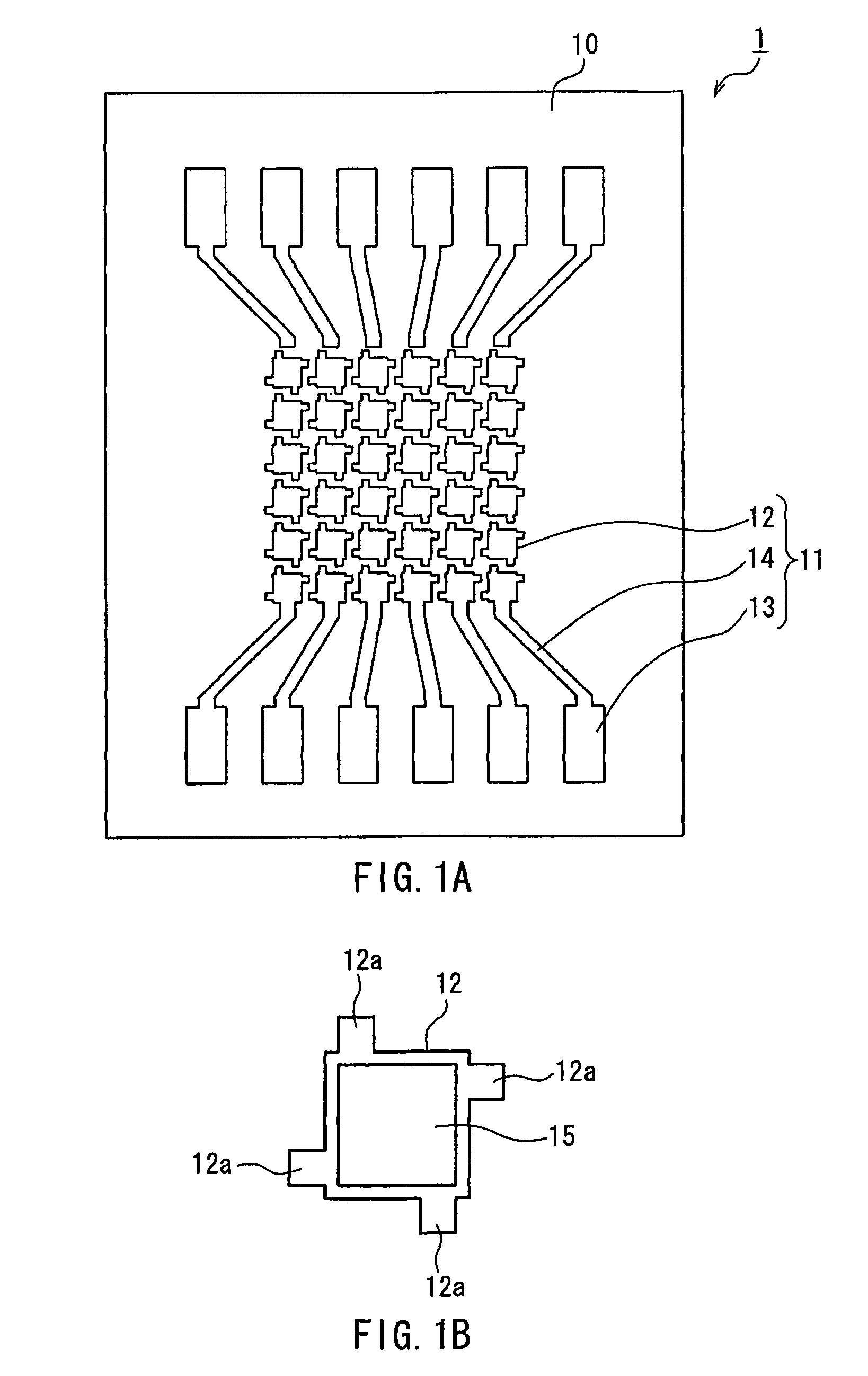
[0030]A mounting board of Embodiment 1 of the present invention will be described by referring to the drawings. FIG. 1A is a plan view of the mounting board of Embodiment 1. FIG. 1B is a plan view of a mount portion included in the mounting board of FIG. 1A, on which a LED chip is mounted.
[0031]As shown in FIG. 1A, the mounting board 1 of Embodiment 1 includes a base material 10 and a conductor pattern 11 formed on the base material 10. The conductor pattern 11 includes a plurality of mount portions 12, a plurality of external connection terminals 13, and a plurality of lead portions 14 for connecting the mount portion 12 and the external connection terminals 13.
[0032]As shown in FIG. 1B, the mount portion 12 has four peripheral portions 12a. When a substantially square LED chip 15 is mounted on the mount portion 12 and viewed perpendicularly to the mounting board 1, the peripheral portions 12a are located outside of each side of the LED chip 15 (see FIG. 1B). Thus, the peripheral p...
embodiment 2
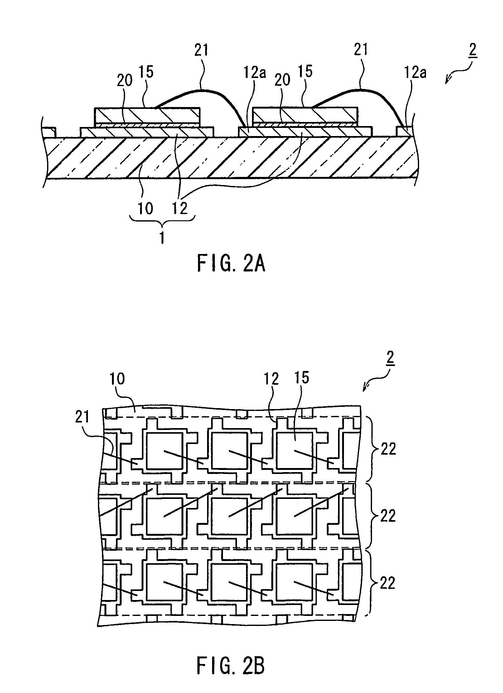
[0033]A light-emitting module of Embodiment 2 of the present invention will be described by referring to the drawings. FIG. 2A is a cross-sectional view of the light-emitting module of Embodiment 2. FIG. 2B is a plan view of the light-emitting module of Embodiment 2, as viewed perpendicularly to a mounting board. The light-emitting module of Embodiment 2 uses the mounting board 1 of Embodiment 1. In FIGS. 2A and 2B, the same components as those in FIGS. 1A and 1B are denoted by the same reference numerals, and the explanation will not be repeated.
[0034]As shown in FIG. 2A, the light-emitting module 2 of Embodiment 2 includes the mounting board 1 and the LED chips 15. The LED chips 15 are die-bonded to each of the mount portions 12 of the mounting board 1 via a conductive adhesive layer 20 made of, e.g., a silver paste. The LED chips 15 are connected in series through the wires 21, the mount portions 12, and the conductive adhesive layers 20. For example, an electrode (not shown) for...
embodiment 3
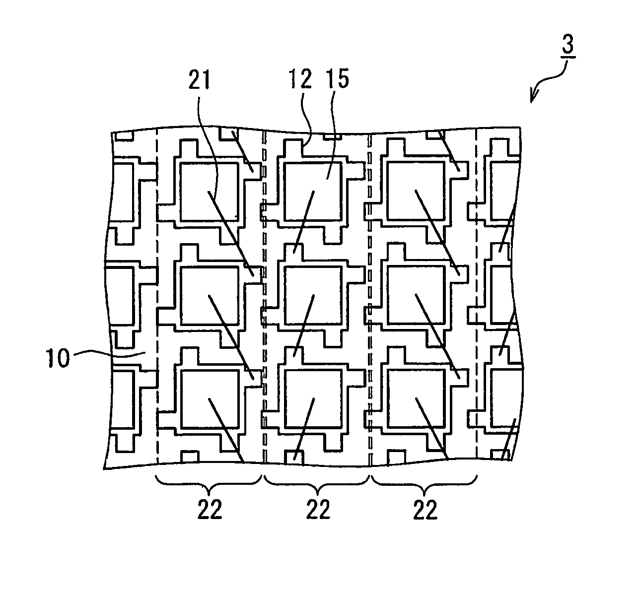
[0038]A light-emitting module of Embodiment 3 of the present invention will be described by referring to the drawings. FIG. 3 is a plan view of the light-emitting module of Embodiment 3, as viewed perpendicularly to a mounting board. In FIG. 3, the same components as those in FIGS. 2A and 2B are denoted by the same reference numerals, and the explanation will not be repeated.
[0039]As shown in FIG. 3, the light-emitting module 3 of Embodiment 3 includes the LED chip units 22 that become longer in the vertical direction of the drawing. In other words, the individual LED chip units 22 are composed of the LED chips 15 connected in series in the vertical direction of the drawing. The other configurations of the light-emitting module 3 are the same as those of the light-emitting module 2. Thus, the light-emitting module 3 also can have an effect comparable to that of the light-emitting module 2.
PUM
 Abstract
Description
Claims
Application Information
 - R&D
- Intellectual Property
- Life Sciences
- Materials
- Tech Scout
- Unparalleled Data Quality
- Higher Quality Content
- 60% Fewer Hallucinations
Browse by: Latest US Patents, China's latest patents, Technical Efficacy Thesaurus, Application Domain, Technology Topic, Popular Technical Reports.
© 2025 PatSnap. All rights reserved.Legal|Privacy policy|Modern Slavery Act Transparency Statement|Sitemap|About US| Contact US: help@patsnap.com